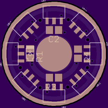
This driver is 22mm in diameter. It is sized specifically for the new monolithic-head (no-pill) F13 flashlights such as the Ultrafire F13. The retaining ring threads on top of the 7135 cases. The 7135’s on top of the board have a setback such that the cases should clear the ledge inside the head, although the tabs may not. This should ensure good ground contact. I used ~20.5mm for the ledge.
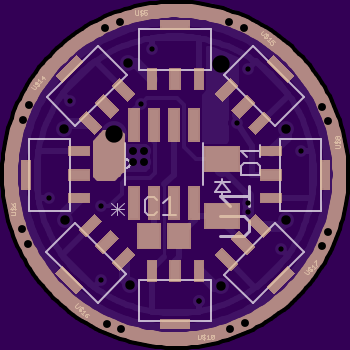
On top of the board is space for the MCU, an SOD-123 package Zener diode, and a 0805 package offtime cap. On the bottom of the board are places for a 0805 voltage divider, a 0805 smoothing cap for Vcc, and a protection diode or 200Ohm resistor. The copper pour in the center is 8mm in diameter, but the exposed copper is only 7.5mm – scrape if you need that little bit extra!
Two special 7135 placements must be considered:
- one for the GND trace for the smoothing cap – there are 4 possible choices
- one for the GND trace for the top of the board – there are 2 choices and both are on top of the board
If you don’t want to use those placements you must manually bridge GND.
UPDATE:
See post #38 for v016 (initial release) and pictures of my 12*7135 build. And see post #54 for v021, the current version.
Still fine, still on a break. One day I’ll catch up with you folks! previous wight catchup
list of my drivers & variants (A17DD, FET+1 stuff, WIP stuff, etc)
Here are the gerbv screenshots:
Still fine, still on a break. One day I’ll catch up with you folks! previous wight catchup
list of my drivers & variants (A17DD, FET+1 stuff, WIP stuff, etc)
C1 will make it VERY difficult to program the ATtiny13 on board
Is that the ground pin for off time memory for STAR firmware?
Otherwise…very very nice design!
Oh and VIAs for ground rings (I use .3302 for those)
16*7145…6A…wow!!!
Do you usually leave the sharp corners on the traces, when I worked on Mattaus’s designs he and I both put small angular reliefs at the sharp corners
Yes, that cap is for offtime STAR firmware. Unfortunately I’m sort of out of space to put it anywhere else and still look all cool.
Thanks for the compliments and thanks for taking a look!
Still fine, still on a break. One day I’ll catch up with you folks! previous wight catchup
list of my drivers & variants (A17DD, FET+1 stuff, WIP stuff, etc)
umm…where is the + and – pads for the wires?
I do need to add those GND vias, totally forgot about that.
Mattaus is a stickler for rounding corners, but as far as I know there are only two reasons to make nice corners:
Since we have guaranteed tolerances for these I don’t care about fab issues. None of our signals are delicate.
Still fine, still on a break. One day I’ll catch up with you folks! previous wight catchup
list of my drivers & variants (A17DD, FET+1 stuff, WIP stuff, etc)
Being the off-time cap it’ll be ok there since you have to remove it to flash anyway. I’m glad it’s there, not that it’s hard to out it between the pin and ground but it’s always nice to have a real pad for it. Looks good, I have a light that needs a 22mm driver, I have a contact board ordered but I’d love to order a set of these for it instead and test it, if your looking for someone send me the files and I’ll order 3.
RIP SPC Joey Riley, KIA 11/24/14. Now I am become death, the destroyer of worlds.
Yeah, makes fine tuning the traces a pain but make for a cleaner render (but makes your head hurt from all that tweaking, re-tweaking, and tweaking some more)
either way, once it’s done it will be a POWERHOUSE of a driver…gonna make those XM-L’s cry for mamma
This will go into a F13 and other 22mm rigs right…I got mine in today
ah…forgot about that
And I guess if you get a good off time build you probably won’t be reflashing that often huh?
Yeah, that’s a minor problem…
Still fine, still on a break. One day I’ll catch up with you folks! previous wight catchup
list of my drivers & variants (A17DD, FET+1 stuff, WIP stuff, etc)
This version has:
I haven’t gotten things 100% worked out with where I’m removing the solder mask for LED- and LED+.
Still fine, still on a break. One day I’ll catch up with you folks! previous wight catchup
list of my drivers & variants (A17DD, FET+1 stuff, WIP stuff, etc)
First set is on the May 04 panel!
RIP SPC Joey Riley, KIA 11/24/14. Now I am become death, the destroyer of worlds.
tStop on minus pad
need – and + on tDocu
And I usually make the identifiers .6~.8 but that’s just me (yeah..nitpicky I know)
And need a BLF on it somewhere
I did mention that in post #10. There’s plenty of copper there to solder to. I’ll probably leave both pads covered in the next version and remove the mask from at least part of the two big vias. If someone wants to solder to the small 1×1mm surface area they just need to scrape.
Still fine, still on a break. One day I’ll catch up with you folks! previous wight catchup
list of my drivers & variants (A17DD, FET+1 stuff, WIP stuff, etc)
Identifiers? The GND vias are 0.5mm because that’s what fits.
Still fine, still on a break. One day I’ll catch up with you folks! previous wight catchup
list of my drivers & variants (A17DD, FET+1 stuff, WIP stuff, etc)
The tDocu letters R1, U1, the white letters on the silk screen (identifiers ???)
Still a pretty darn cool design
Oh, gotcha. I just ignore that stuff until the rest is sorted out.
Still fine, still on a break. One day I’ll catch up with you folks! previous wight catchup
list of my drivers & variants (A17DD, FET+1 stuff, WIP stuff, etc)
Is R1 a resistor or diode?
Three Tanna leaves to give him life, nine to give him movement. But what if he eats the whole bag?
Scott
Depends on whether D1 is populated with a Zener diode or not.
Still fine, still on a break. One day I’ll catch up with you folks! previous wight catchup
list of my drivers & variants (A17DD, FET+1 stuff, WIP stuff, etc)
I was confused why there is a zener diode for a single cell flashlight driver. I'm guessing you're designing in options for use in other lights later on?
It looks good.
Well, really just for flexibility. Mainly as you say – in case someone wants to use it in a different light. Also though, someone might choose to run the F13 on a pair of 18350. Or if some battery manufacturer ever made a good 26350 :drool:
Still fine, still on a break. One day I’ll catch up with you folks! previous wight catchup
list of my drivers & variants (A17DD, FET+1 stuff, WIP stuff, etc)
Thanks, I couldn’t reconcile the print and the pictogram.
Don’t tease me bro.
Three Tanna leaves to give him life, nine to give him movement. But what if he eats the whole bag?
Scott
What did I change? I don’t know. I spent too much time tweaking stuff tonight.
Just for fun, here are the drills:
Still fine, still on a break. One day I’ll catch up with you folks! previous wight catchup
list of my drivers & variants (A17DD, FET+1 stuff, WIP stuff, etc)
I realized that there was no reason for the exposed copper GND ring on the bottom of the board in this application, and it’s actually a pain because it prevents you from easily aligning the 7135’s. So I put the mask back over that and removed the mask from the vias because I think that looks cool and why would I need a better reason than that
I also realized that I do not have a polarity marking for D1. Oops. Hopefully that gets fixed in a future revision. Maybe I’ll feed the voltage divider directly from BAT+ in a future revision too.
My first set is on the June 06 panelStill fine, still on a break. One day I’ll catch up with you folks! previous wight catchup
list of my drivers & variants (A17DD, FET+1 stuff, WIP stuff, etc)
Very nice!
The drills looks like the starry sky
Those thru hole wire positions are nice…huge thick wires can be used…excellent
What is the 7135-A and B for…not populating all the 7135 positions for zener builds??
Thanks! Starry sky was my first thought as well, I was paying attention to something else and it took me off guard when I scrolled past the drills on Oshpark.
Still fine, still on a break. One day I’ll catch up with you folks! previous wight catchup
list of my drivers & variants (A17DD, FET+1 stuff, WIP stuff, etc)
All the 7135’s on the bottom are grounded…
I’m a bit confused…the center pin on the 7135 has a solid connection all the way thru underneath to the tab on the back…so the bottom side with the spring, when you solder them down they are all automatically grounded
And I see the thru holes from the bottom go to the top sides, so they too would be grounded…correct?
And on the top side, you could put a simple trace from the back pad to the ground ring under the solder stop
Ah, but if they ain’t there in those A and B position…no under the chip ground path…NOW I see it…DUH! (smack head, coulda had a V8 moment
)
Not everybody wants 16*7135 inside these little flashlights! I imagine that this PCB will generally be used with something in the range of 4*7135 to 12*7135.
There are two portions of the circuit which required ground paths and do not have a direct connection to the main GND ring.
C1 is the easiest example to look at. It obviously has no ground connection unless one of the 7135-A placements is populated. We are using the “solid connection” you mentioned as a zero-ohm jumper to get past the blocking trace!
Since I used a complete ring on both sides there is actually space to break the PWM and LED+ rings and allow a path to GND. Maybe I’ll do that. Personally I like complete rings and I see no scenario where at least one position on both A and B wouldn’t get populated.
Still fine, still on a break. One day I’ll catch up with you folks! previous wight catchup
list of my drivers & variants (A17DD, FET+1 stuff, WIP stuff, etc)
Understood…thanks
Heh, now I see where you figured it out as I was typing. It’s not the most intuitive thing in the world. I’d say it’s one of those situations where it’s way easier to figure it out when it was your own plan to start out with.
Still fine, still on a break. One day I’ll catch up with you folks! previous wight catchup
list of my drivers & variants (A17DD, FET+1 stuff, WIP stuff, etc)
I know nothing about designing PCB's, but I really like the clean, elegant design of your board. No spaghetti traces zig zagging around. All are short and direct.
Pages