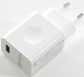
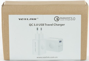
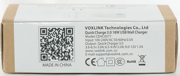
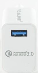
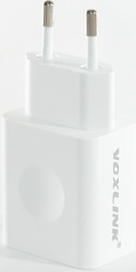
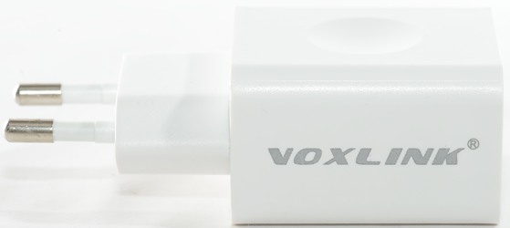
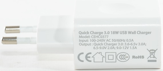
Voxlink 18W QC3 CEHC0377
Official specifications:
-
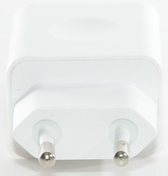
Input: 100V-240V
-
Interface: 1 USB port
-
Output: 3.6-6.5V 3.0A, 8.5-9V 2.0A, 9.0-12V 1.5A
-
Working temperature: 0 - +65 °?
-
Storage temperature:
40+85 °? -
Fire and shatter proof material
I got it from a ebay dealer: iremoteworld
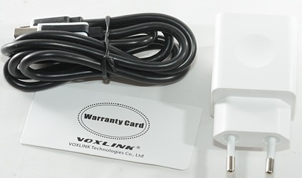
The box includes the usb charger, a thick usb cable and a warranty card.
Measurements
-
Power consumption when idle is 0.04 watt
-
Output is coded as QC3
-
Minimum QC3 voltage is 3.56 volt
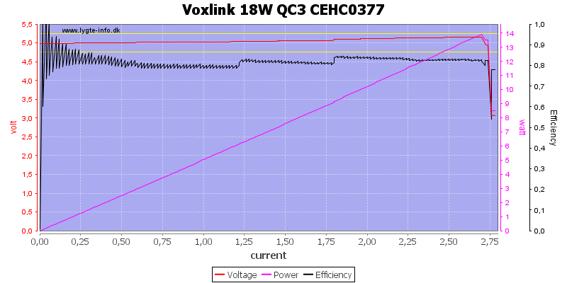
The output is rated for 3A but cannot deliver more than 2.7A.
The output voltage will increase with load to compensate for cable losses.
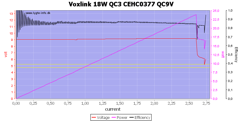
At 9V the current is slightly down, but over specifications.
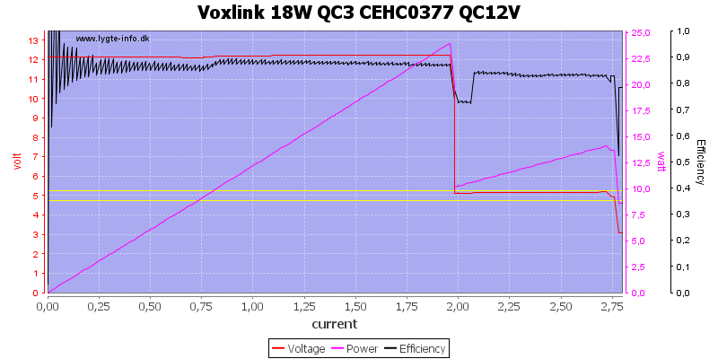
Same with 12V, it is rated for 1.5A ,but can deliver 2A.
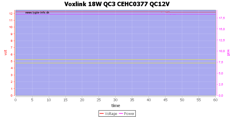
I could draw 1.5A for 1 hour, without any problems.
The temperature photos below are taken between 30 minutes and 60 minutes into the one hour test.
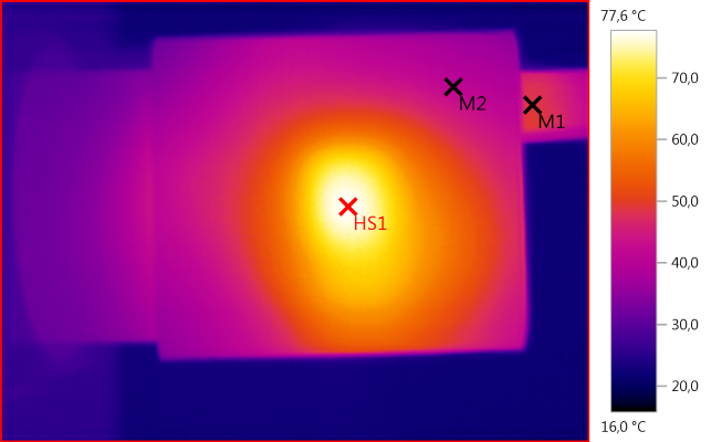
M1: 48,6°C, M2: 41,6°C, HS1: 77,6°C
HS1 is the transformer.
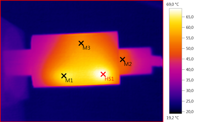
M1: 63,9°C, M2: 49,9°C, M3: 54,9°C, HS1: 69,0°C
HS1 is the rectifier transistor.
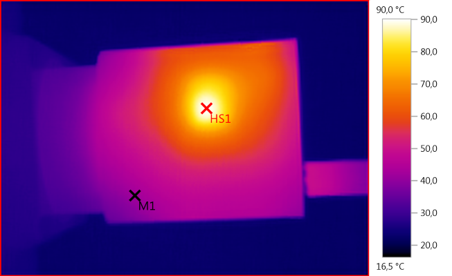
M1: 42,0°C, HS1: 90,0°C
HS1 is the controller chip and the transformator.
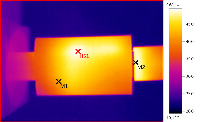
M1: 42,0°C, M2: 48,3°C, HS1: 49,4°C
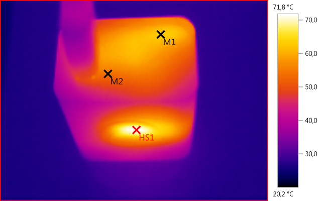
M1: 63,0°C, M2: 53,8°C, HS1: 71,8°C
HS1 is the transformer and M1 is the rectifier transistor.
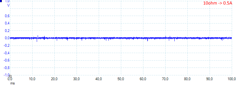
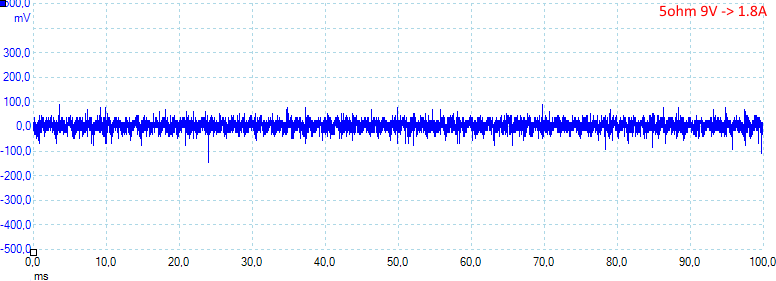
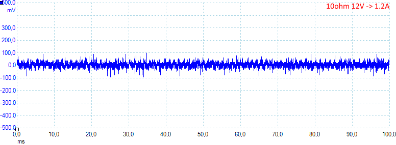
Noise at 0.5A load is 11mV rms and 177mVpp
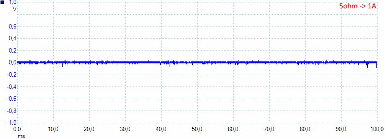
Noise at 1A load is 13mV rms and 177mVpp
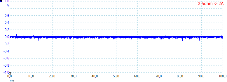
Noise at 2A load is 19mV rms and 220mVpp
Noise at 2A load is 19mV rms and 255mVpp
Noise at 2A load is 19mV rms and 233mVpp
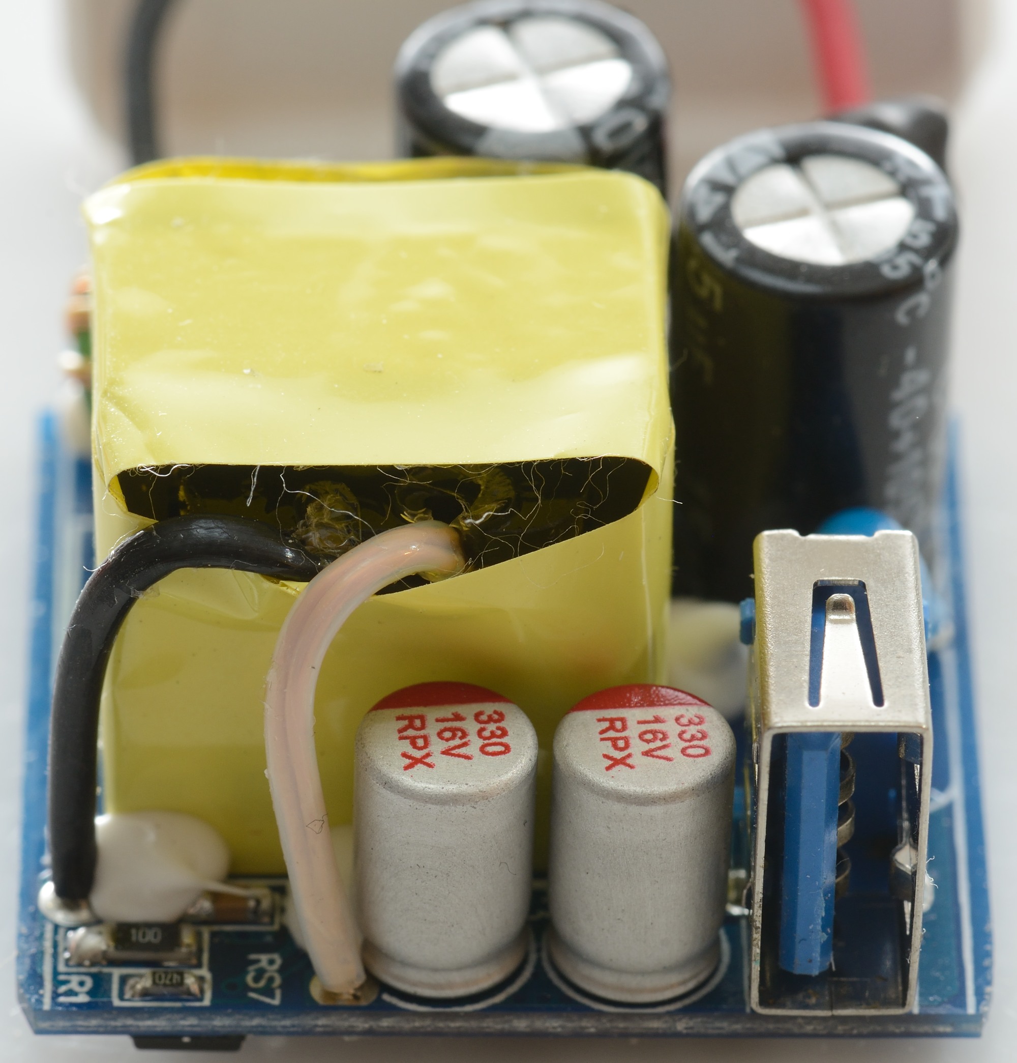
Tear down
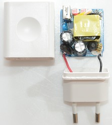
I could break the glue with my vice and then break it open without any damage.
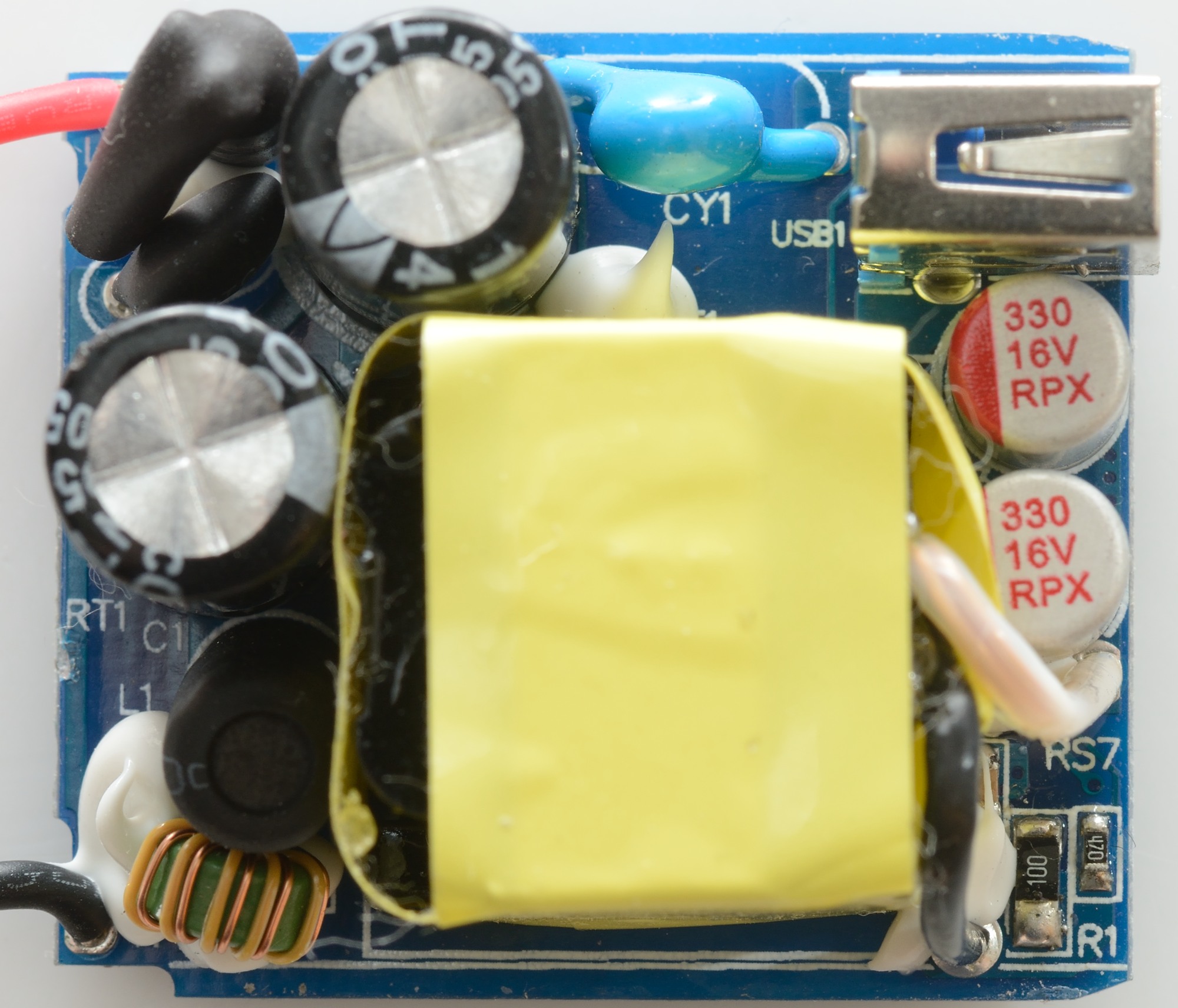
At the mains input red wire there is a fuse and a inrush protection, at the black wire there is a common mode coil and a inductor.
CY1 is the safety capacitor.
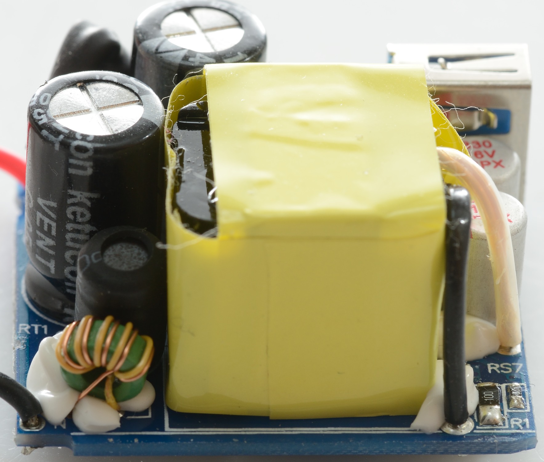
From this side the common mode could and the inductor can be seen.
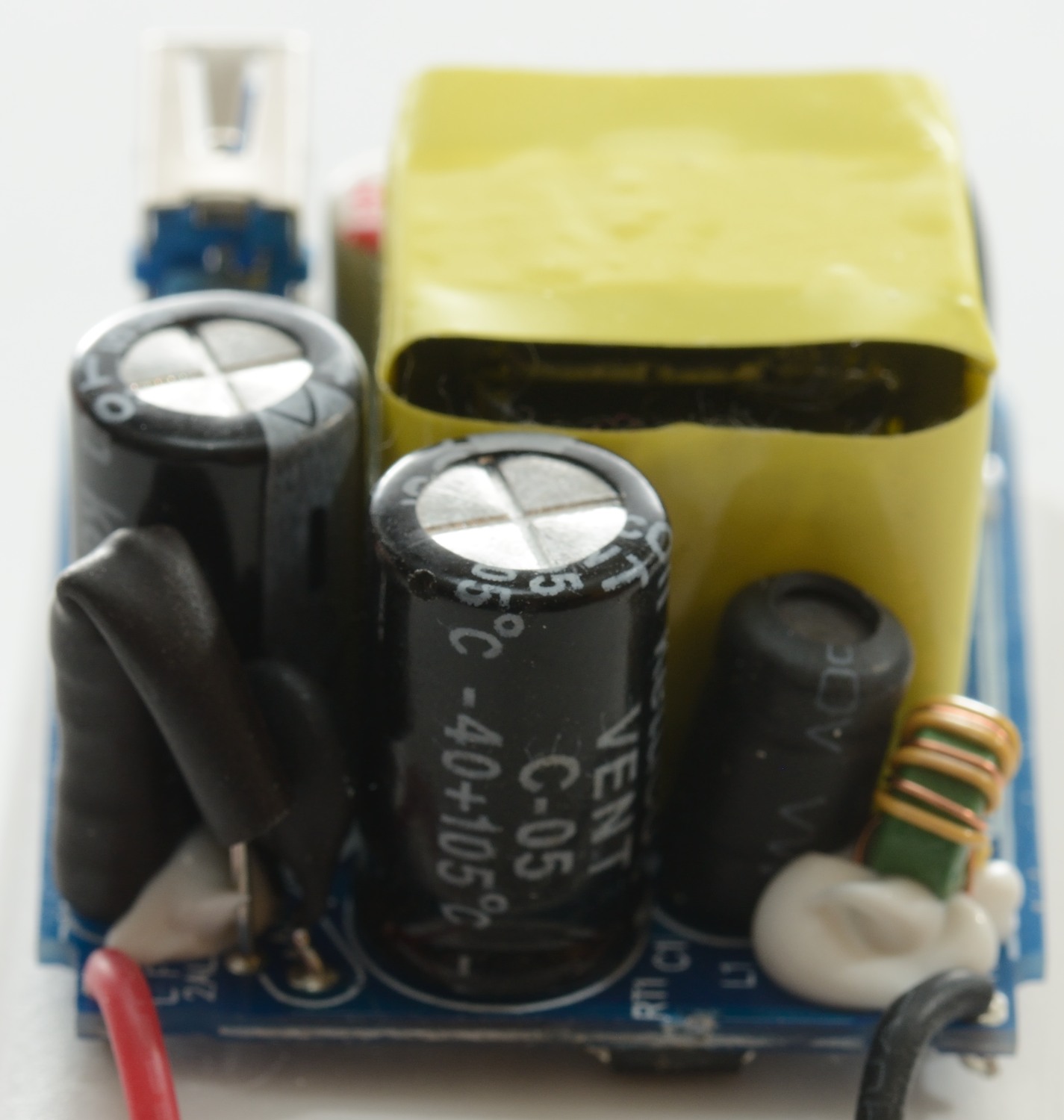
Behind the fuse the inrush pretection can be seen, it is a black disc.
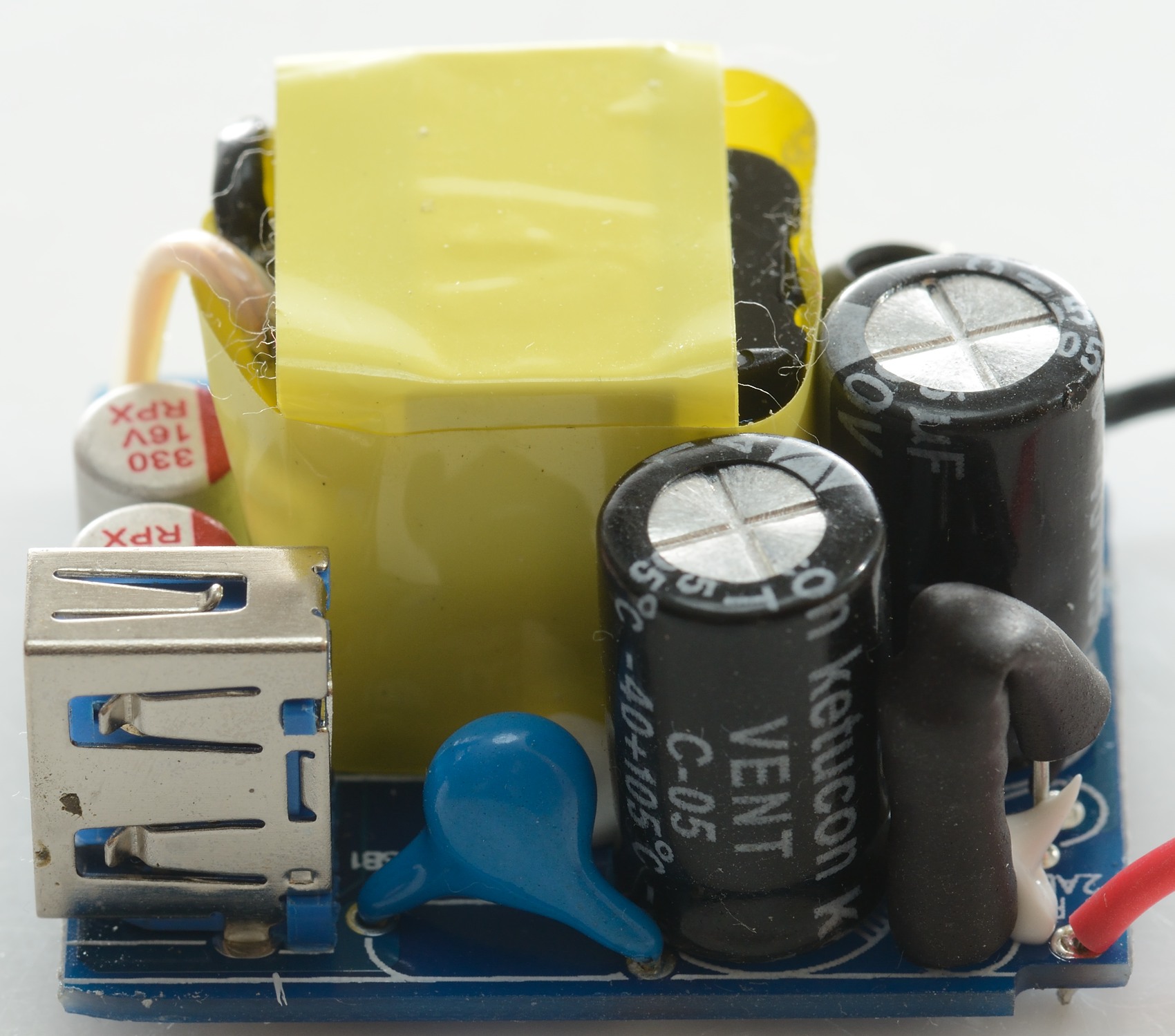
The blue safety capacitor can be seen behind the usb connector.
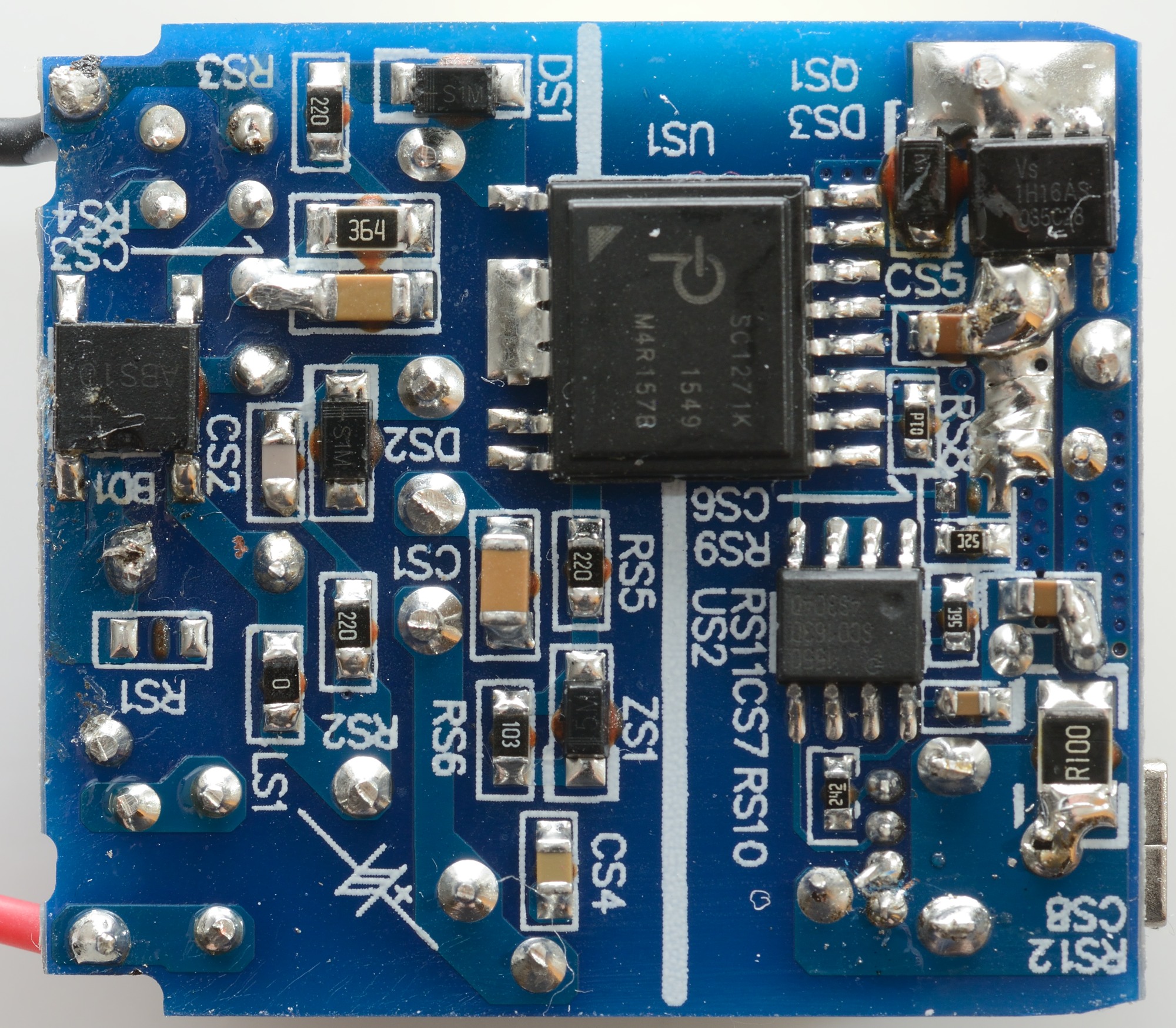
At the mains input the bridge rectifer (BD1) is placed. The large chip (US1) is the switcher and also contains feedback and synchronus rectifier control. The chip with most legs soldered together is the rectifier transistor.
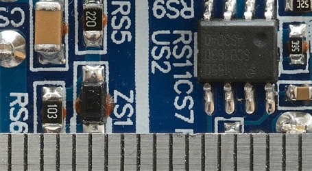
The other 8 pin chip (US2) is the Quick Charge 3 controller (Probably SCD 1630, but I could not find a datasheet)
Notice the large R100 at the output, it is probably used for current limiting.
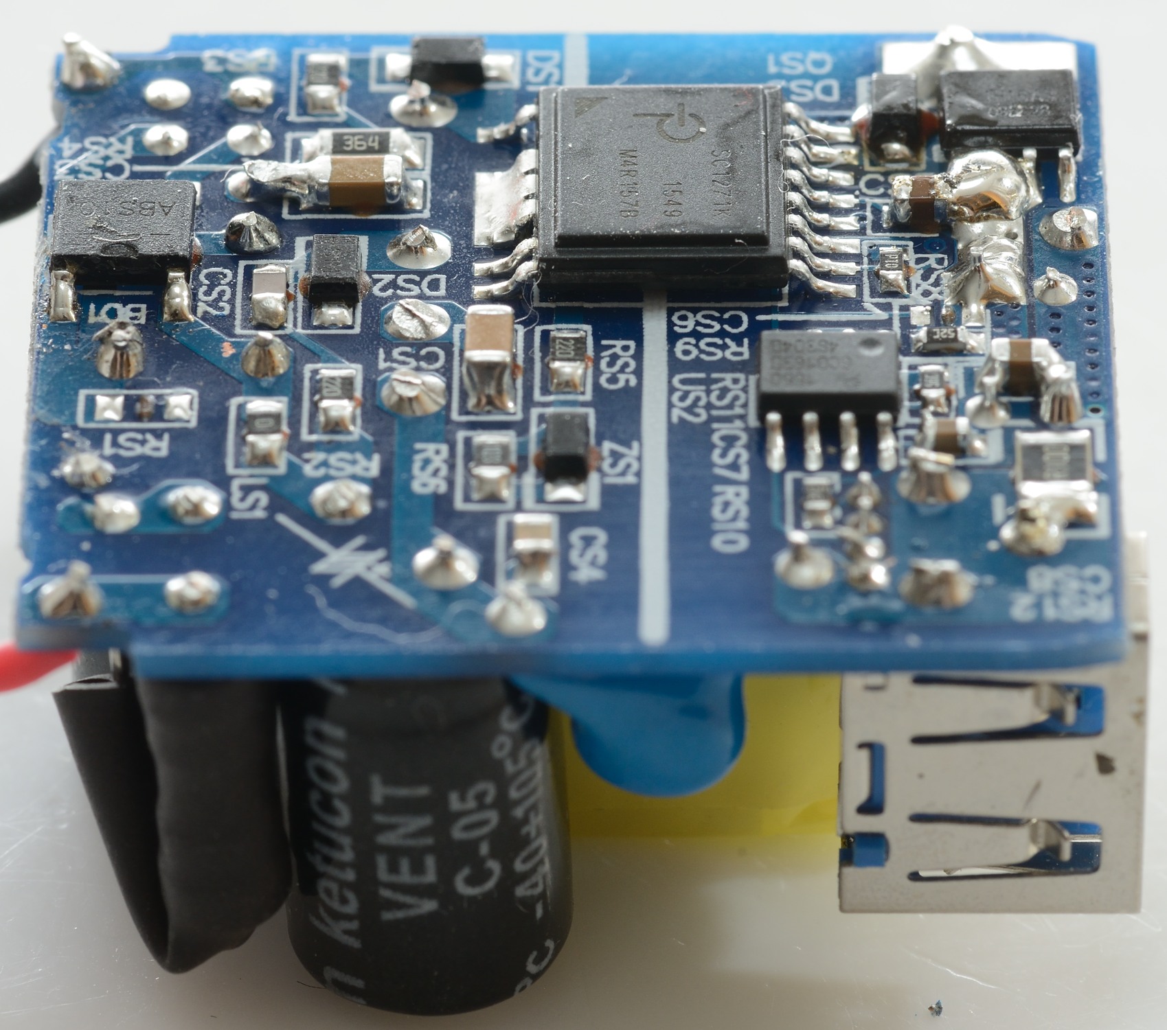
The distance between mains and low volt side is acceptable, it is just above 6mm.
Testing with 2500 volt and 5000 volt between mains and low volt side, did not show any safety problems.
Conclusion
I you need quick charge this looks like a good charger with support for both QC2 and QC3 (QC2 is implied in QC3). I doubt the slightly lower output current at 5 volt will be a problem.
Notes
Index of all tested USB power supplies/chargers
Read more about how I test USB power supplies/charger