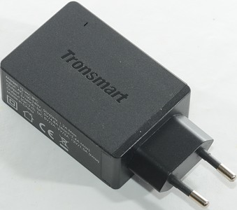
Tronsmart 2 USB + 1 QC2 TS-WC3PC
Official specifications:
-
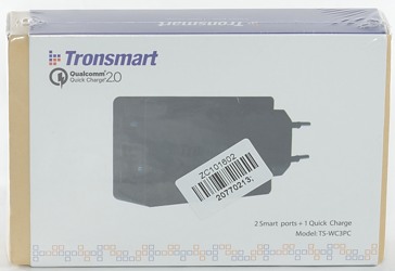
Brand: Tronsmart
-
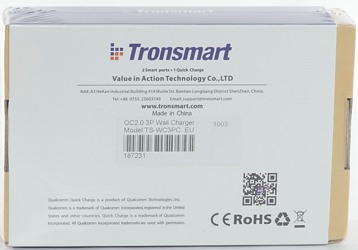
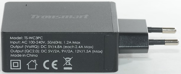
Model: TS-WC3PC
-
Tech: Qualcomm Quick Charge 2.0 / VoltIQ
-
Quantity: 1 Piece
-
Color : Black
-
Input : AC 100-240V 50/60Hz 1.2A
-
Charging Output & Power(VoltIQ ): 5V/4.8A(Maximum 2.4A Each) 24W
-
Power: 42W
-
Charging Output & Power(Quick Charge ): DC 5V/2A, 9V/2A, 12V/1.5A & 10W/18W(Max)
-
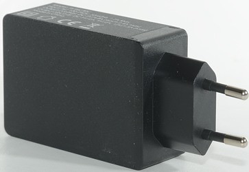
Dimension: 108.3X48.3X26.4MM
-
Plug Type: US, EU
-
Net weight: 103g
I got it from ebay dealer finetech007
I got it in a brown cardboard box with a white wrapper.
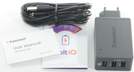
The box contained the charger, user manual, usb cable and a note.
Measurements
-
Power consumption when idle is 0.17 watt
-
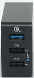
VoltIQ outputs is auto coded with up to Apple 2.4A
-
QC output is QC coded
-
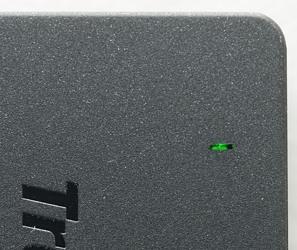
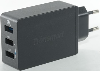
The charger has a green led on one side.
-
The two VoltIQ outputs are in parallel.
The output can deliver lots of current and there is no separate overload protection.
Same on the other VoltIQ output.
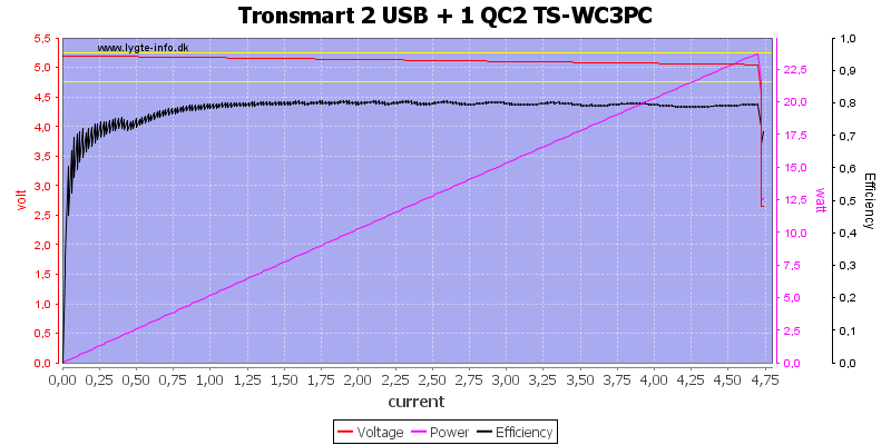
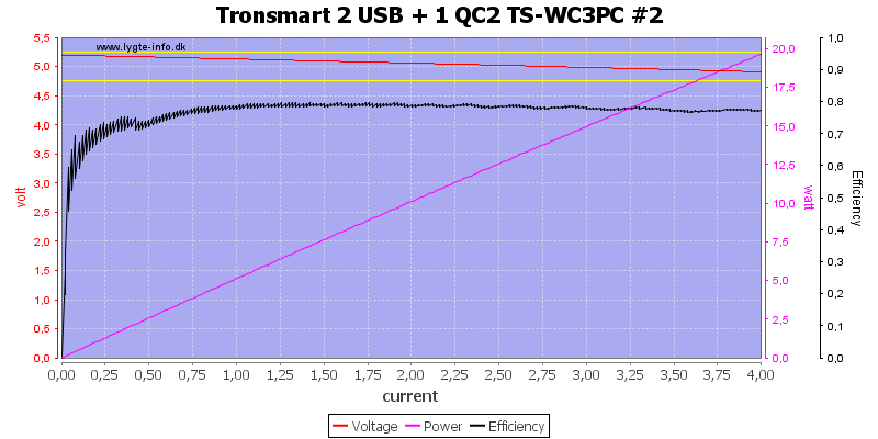
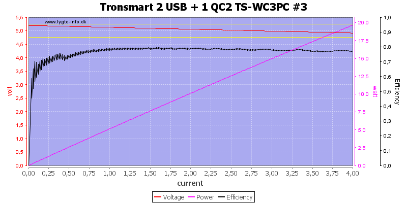
When using them together I can see it has an overload protection at about 4.7A, this is slightly low for a 4.8A rated charger.
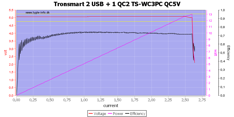
With QC the overload protection is at 2.6A at 5V, this is a much more reasonable value.
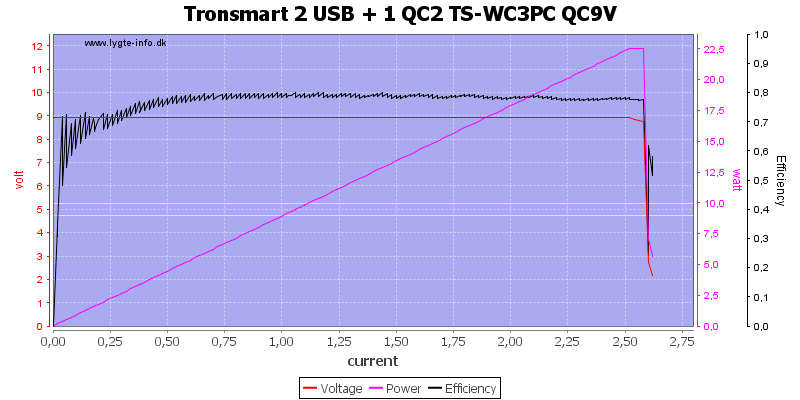
Increasing the voltage do not really change the overload protection.
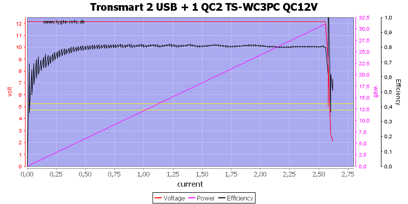
Even at 12V.
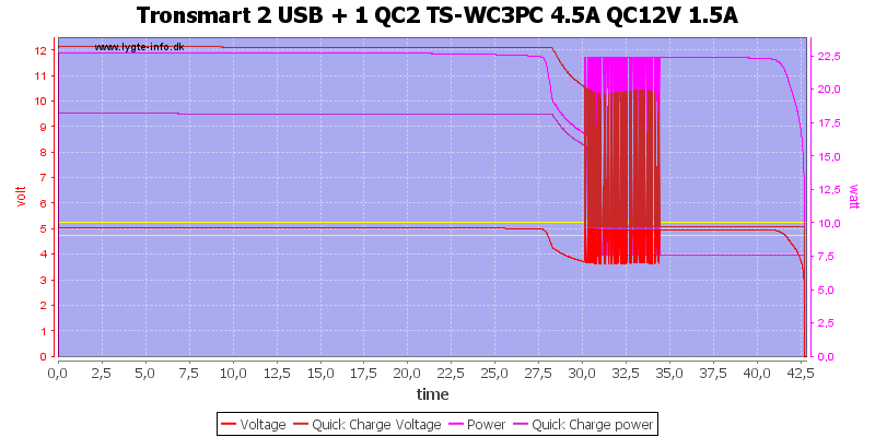
Here I try to run for one hour at maximum rated load, but the charger can only maintain output for 27 minutes.
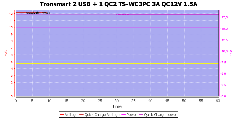
Reducing the current made it possible to run for one hour.
The temperature photos below are taken between 30 minutes and 60 minutes into the one hour test.
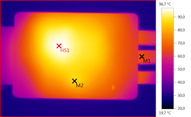
M1: 65,3°C, M2: 86,1°C, HS1: 96,7°C
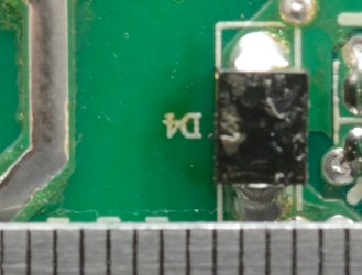
HS1 is the transformer and M2 is the QC rectifier diode (D4).
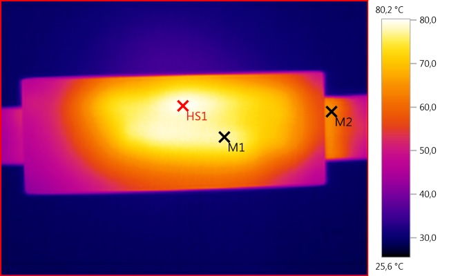
M1: 77,5°C, M2: 63,9°C, HS1: 80,2°C
HS1 is the QC diode and M1 is the QC switcher chip.
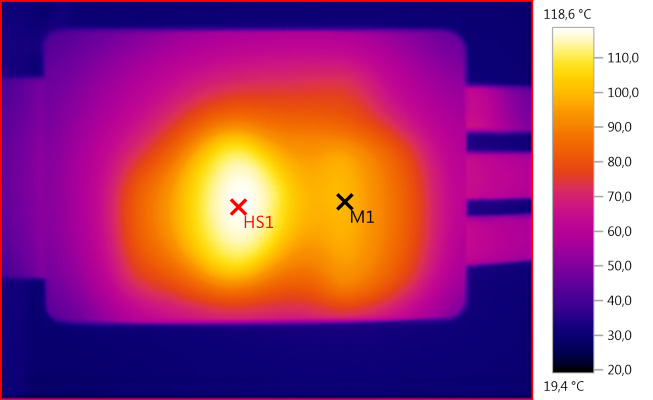
M1: 99,5°C, HS1: 118,6°C
HS1 is the transformer and M1 is the heatsink for the two rectifier diodes.
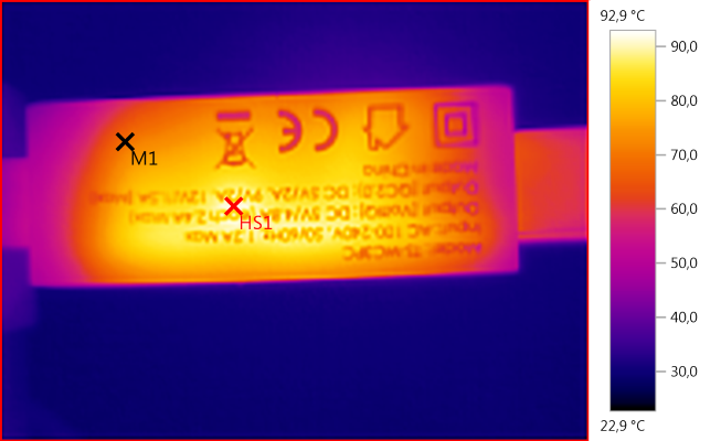
M1: 68,9°C, HS1: 92,9°C
HS1 is the transformer again.
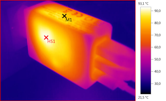
M1: 83,3°C, HS1: 93,1°C
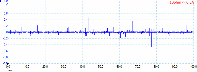
At 0.5A the noise is 24mV rms and 1300mVpp, this is very high peak noise.
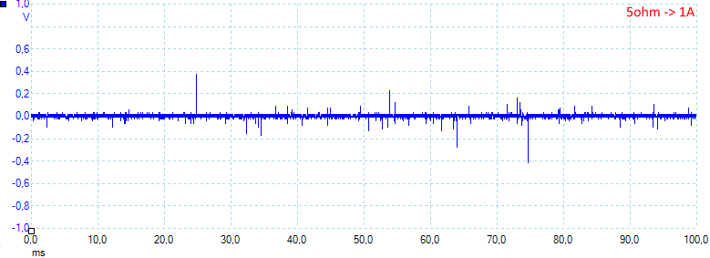
At 1A the noise is 18mV rms and 1300mVpp, this is very high peak noise.
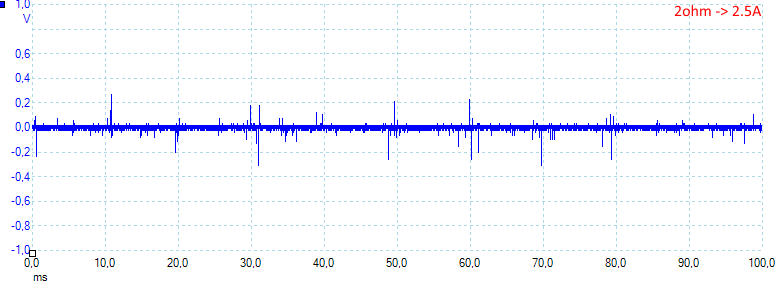
At 2.5A the noise is 23mV rms and 910mVpp
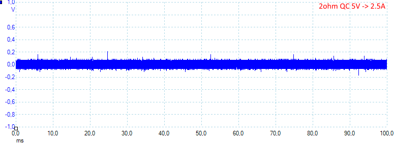
At 5V and 2.5A on QuickCharge the noise is 57mV rms and 626mVpp
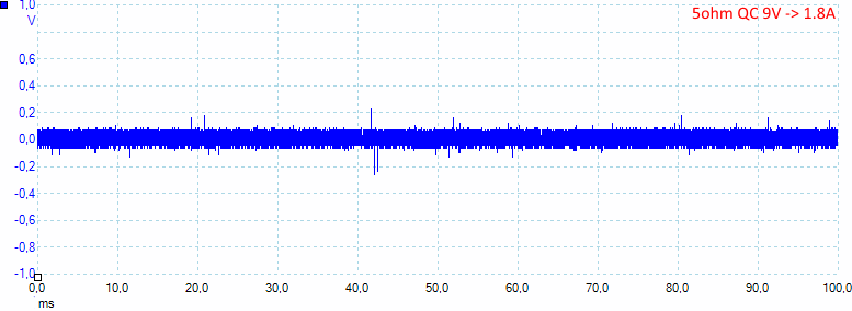
At 9V and 1.8A on QuickCharge the noise is 46mV rms and 660mVpp
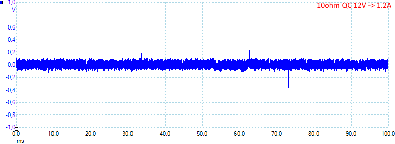
At 12V and 1.2A on QuickCharge the noise is 51mV rms and 820mVpp
Tear down
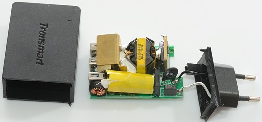
I could not break the glue with a vice or mallet, I had to cut it open.

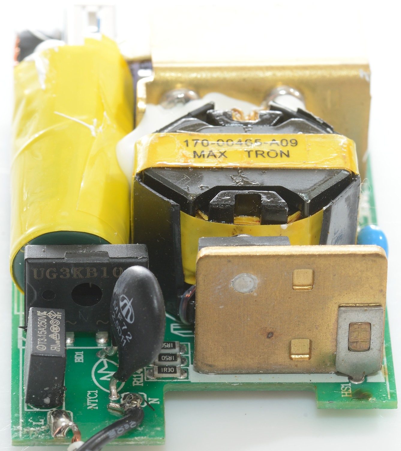
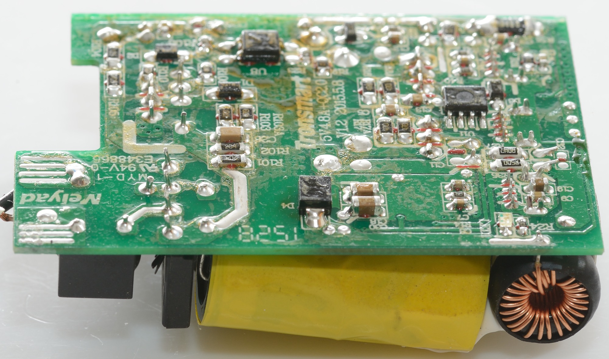
The charger looks very packed, except at the mains input.
At the mains input there is a black fuse and a inrush current protection (NTC1), then a bridge rectifier (BD1). The mains switcher transistor is mounted on the small heatsink (HS1) with the small controller mounted on the other side of the white stuff.
Next to the controller is the safety capacitor.
The other heatsink has two rectifiers for the two secondary windings on the transformer (One for QC, one for VoltIQ).
Beside the QC output is the inductor for the QC switcher.
There is no noise filtering at the mains input.
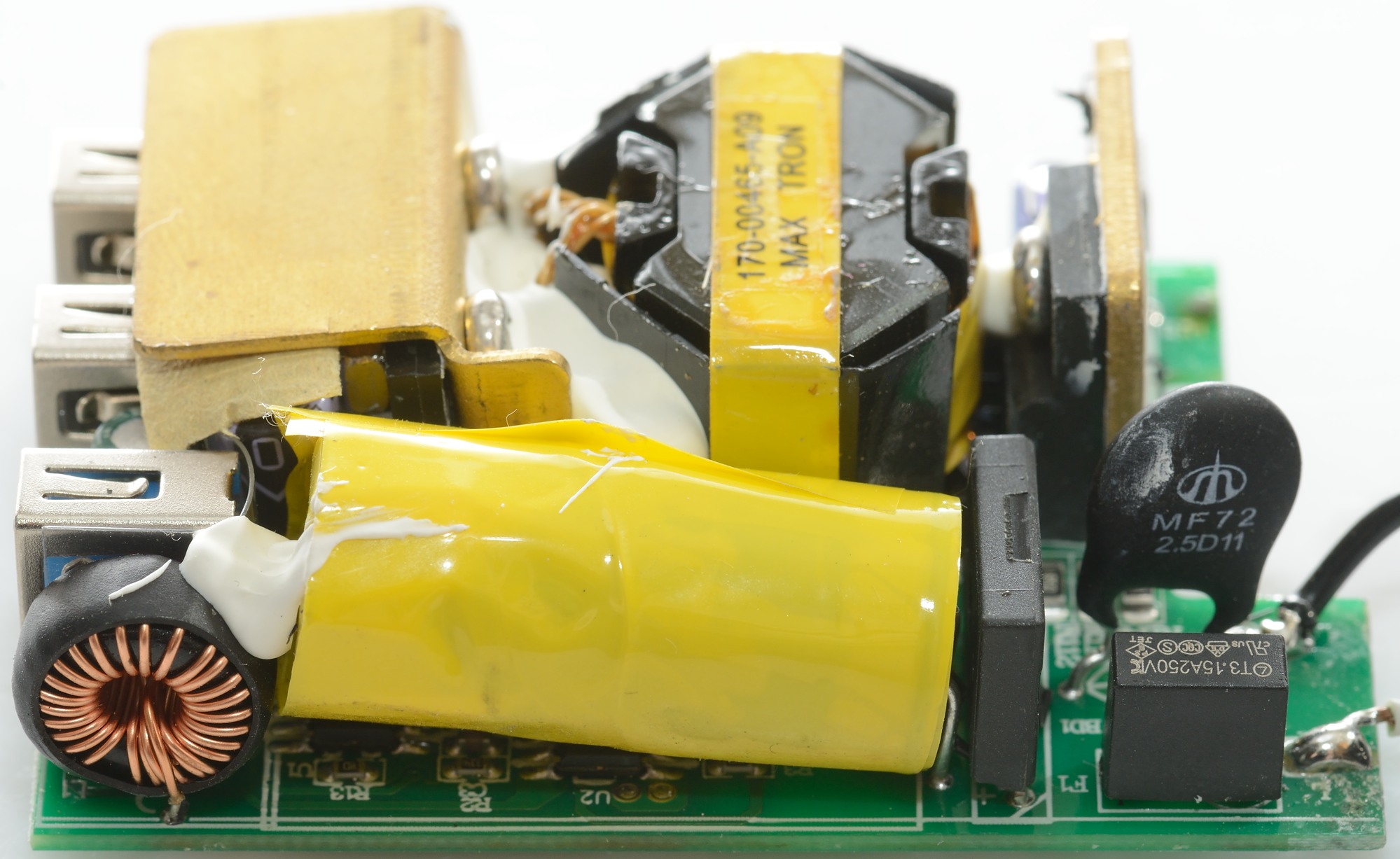
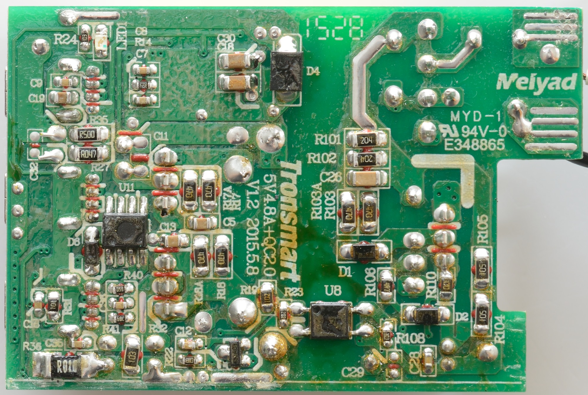
From this side the QC inductor (L1) is easier to see and it can be seen that there is some part under the capacitor with yellow tape. The tape is used to improve isolation, the plastic on a capacitor do usual not have a safety rating, to get around that a layer of yellow tape is added.

From this side the mains switcher controller can be seen together with the safety capacitor.

Here the VoltIQ (i.e. auto coding chip) can be see (U4) between the two usb connectors, next to the QC connector is a 16V capacitor, i.e. it is used for QC.
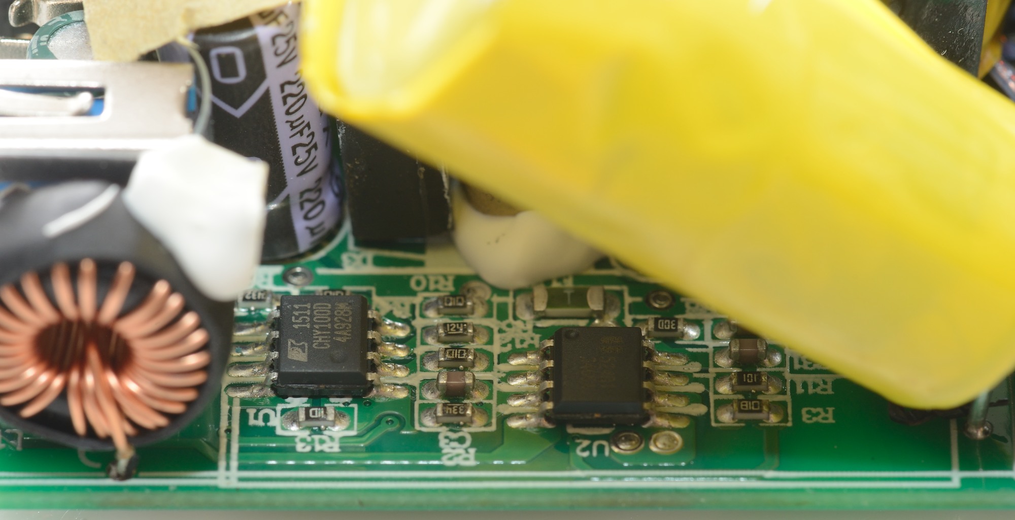
A look under the capacitor. The CHY100 chip is the QC controller, the means the other chip (U2) must be the buck regulator.
Notice the 220uF 25V capacitor, it is the input voltage for the QC buck regulator.
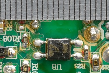
There is some easy parts to guess: The QC rectifier diode (D4), the optocoupler (U8), the 3pin voltage reference next to the optocoupler.
But what is U11, there is no type number on it? I can see two possibilities, either a synchronous rectifier controller, but both rectifiers are diodes, this kills that idea.
Next idea is a OpAmp (Like LM358) used together with all the low ohmic resistors (R010 & R047) to handle current limits.
Creepage distance is above 6mm.
Testing with 2500 volt and 5000 volt between mains and low volt side, did not show any safety problems.
Conclusion
The charger cannot deliver the rated current, this is not really a big deal, very few people need to charge 3 pads simultaneous and it can easily handle two, but due to the high temperature it will cost some lifetime.
The peak noise is way too high
I will only rate this charger acceptable.
Notes
Index of all tested USB power supplies/chargers
Read more about how I test USB power supplies/charger
How does a usb charger work?


