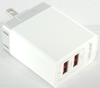
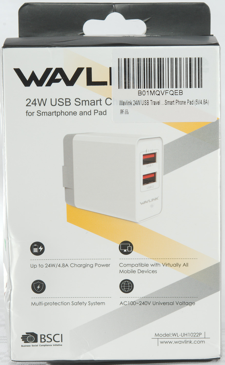
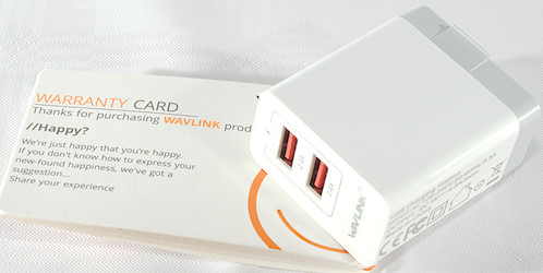
Wavlink 24W-4.8A Quick Charger
Official specifications:
-
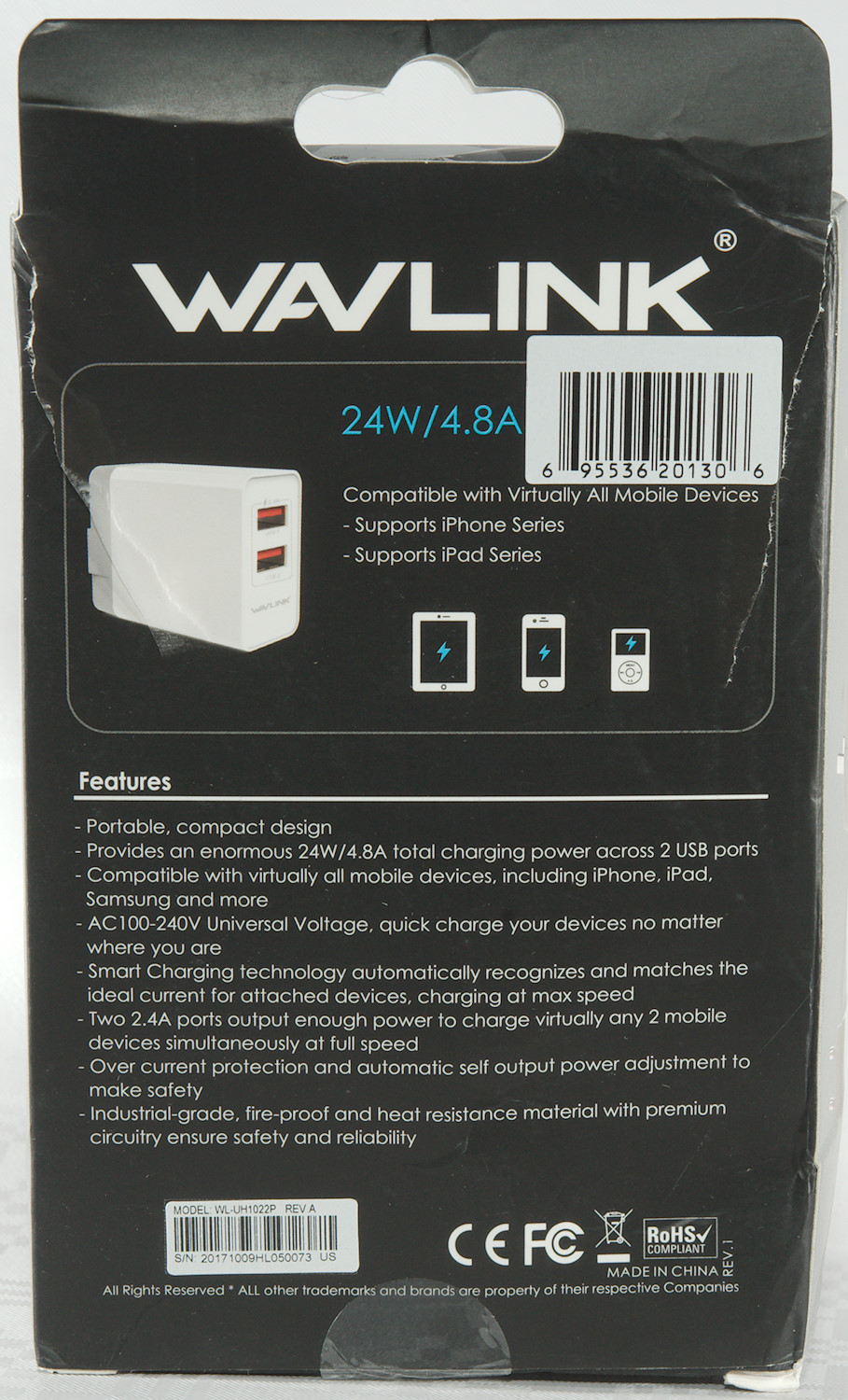
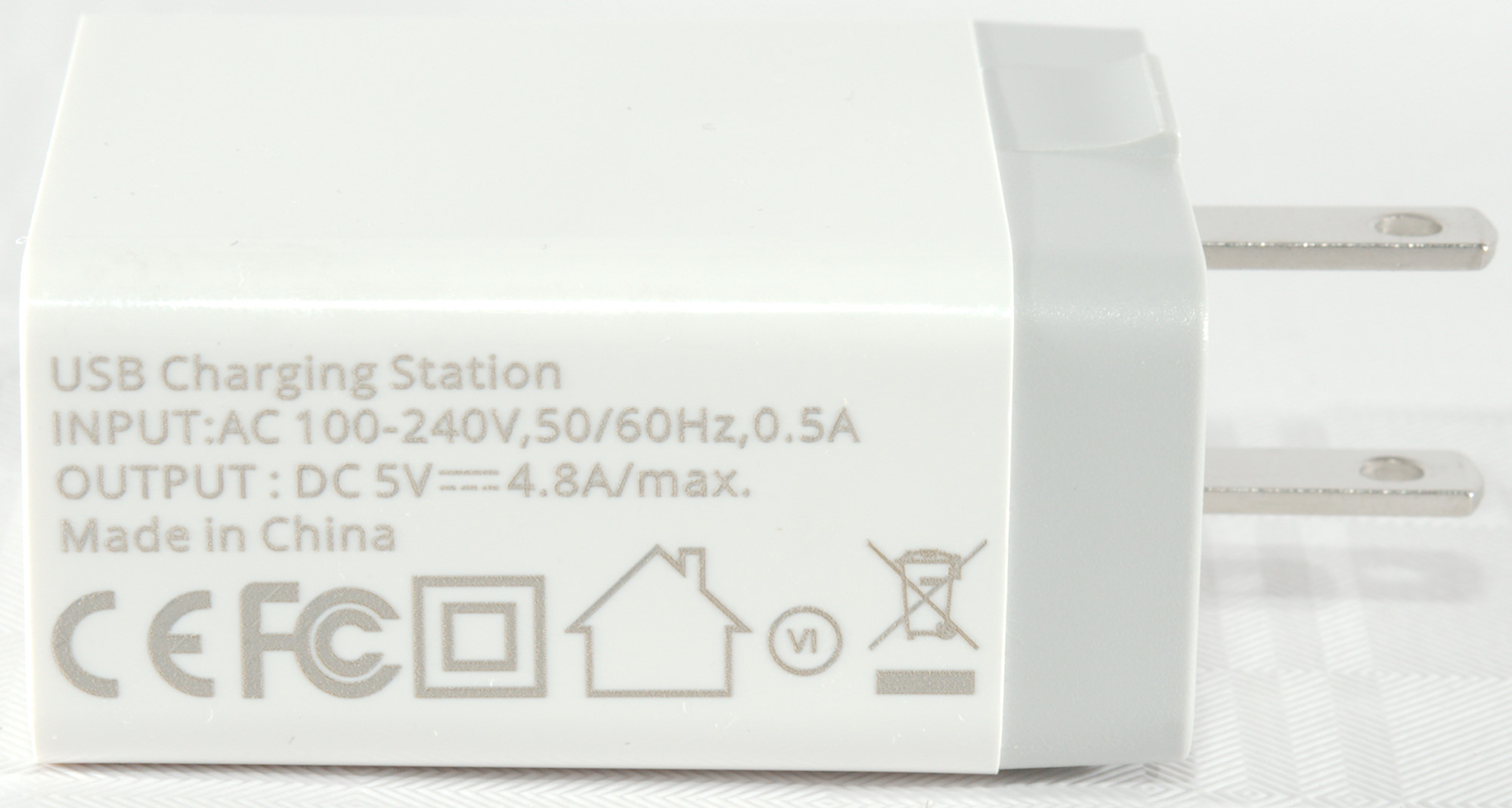
Input Rating: AC100-240V 50/60Hz 1A
-
Input frequency: 50/60Hz
-
Rated output value: DC5V / 4.8A(Port Max 2.4A)
-
Output power: 24Watt
I got it from ebay dealer sinobry

Measurements
-
Power consumption when idle is 0.06 watt
-
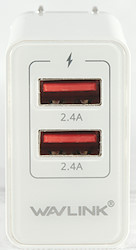
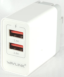
Both USB output is auto code with Apple 2.4A, Samsung and DCP
-
USB outputs are in parallel.
-
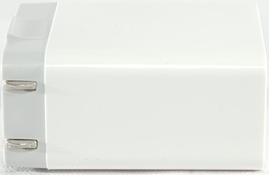
Weight: 66.6g
-
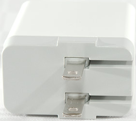
Size: 54.4 x 46.1 x 27.8mm
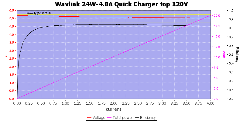
The top port can deliver more than 4A.
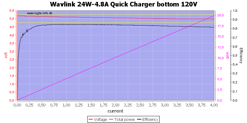
It is the same with the bottom port, i.e. there is no individual overload protection.
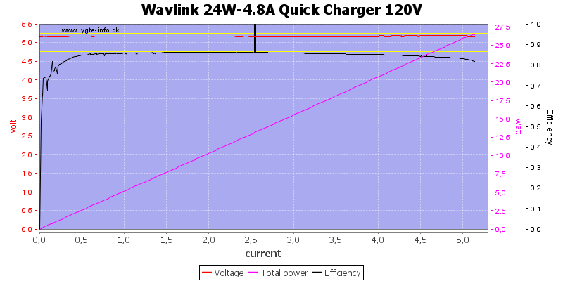
When run together the maximum is slightly above 5A, this matches fine with a 4.8A rating, but it way to much for a single USB port.
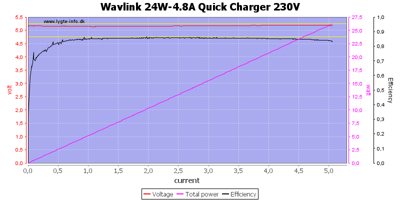
The overload limit goes slightly down at 230V.
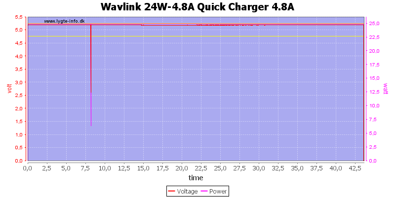
The charger could not deliver 4.8A for one hour, it shut down after 43 minutes.
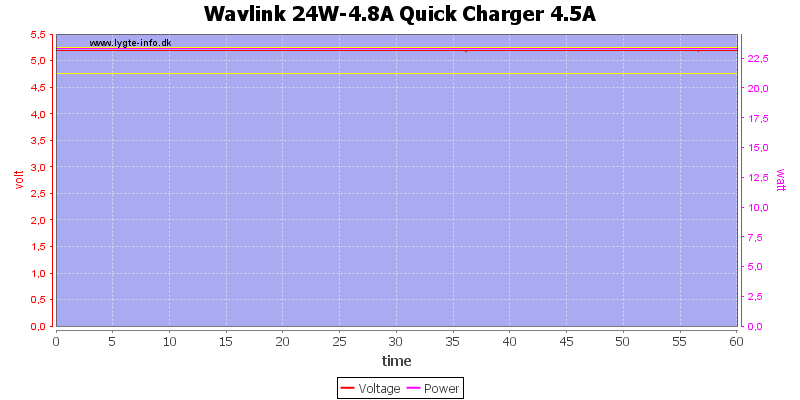
After reducing current to 4.5A it could easily run for 1 hour.
The temperature photos below are taken between 30 minutes and 60 minutes into the one hour test.
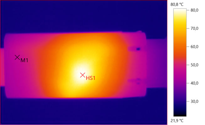
M1: 46.6°C, HS1: 80.8°C
HS1 is the transformer.
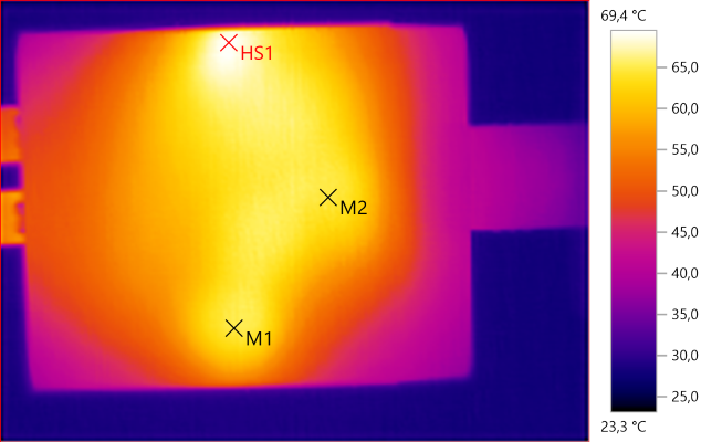
M1: 65.0°C, M2: 64.6°C, HS1: 69.4°C
Again HS1 is the transformer, M1 and M2 is the two input smoothing capacitors.
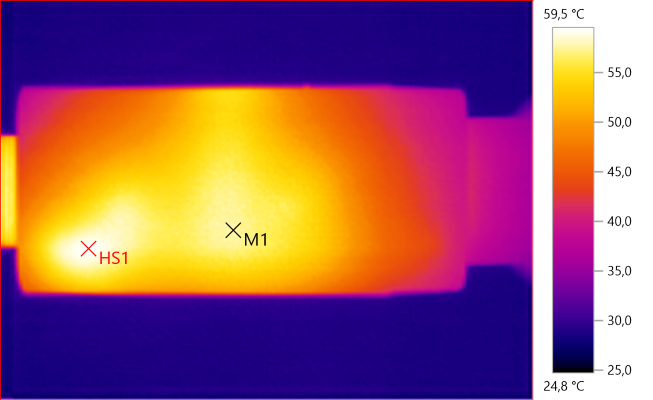
M1: 57.6°C, HS1: 59.5°C
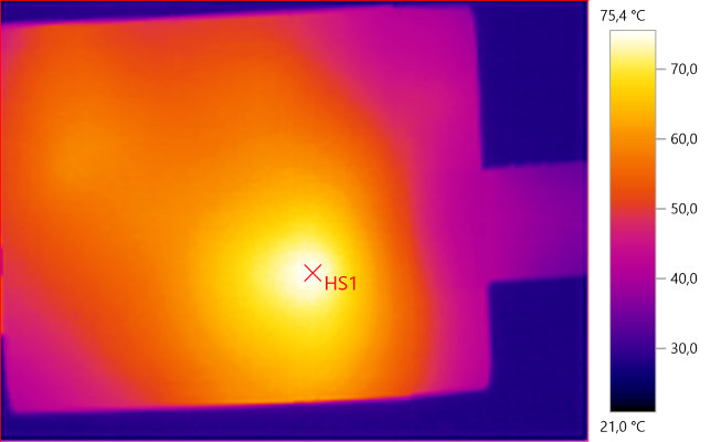
HS1: 75.4°C
HS1 is most either the transformer hear or from the snubber network
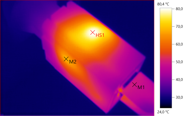
M1: 49.3°C, M2: 68.4°C, HS1: 80.4°C
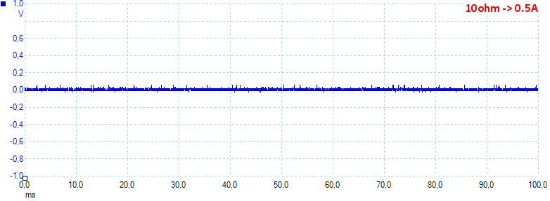
At 0.5A the noise is 11mV rms and 101mVpp.
At 1A the noise is 20mV rms and 184mVpp.
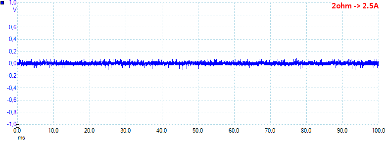
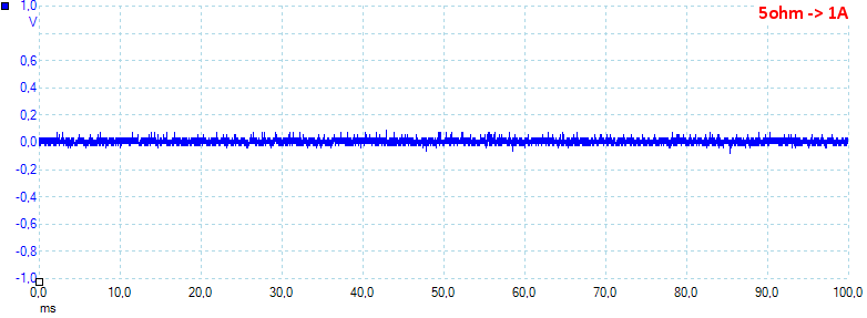
At 2.5A the noise is 23mV rms and 213mVpp.
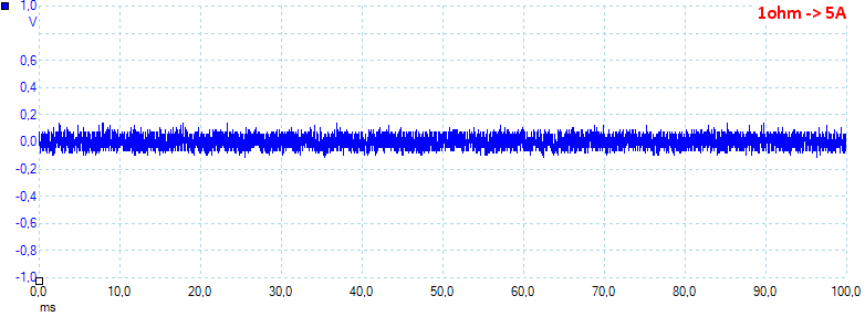
At 5A the noise is 43mV rms and 287mVpp, all very low noise values.
Tear down
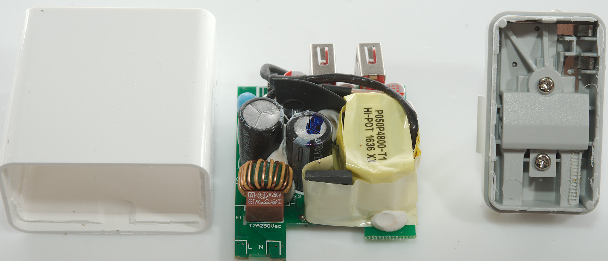
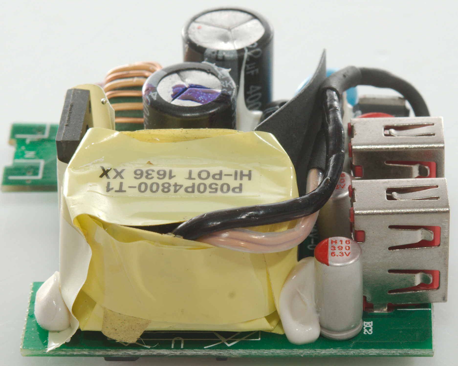
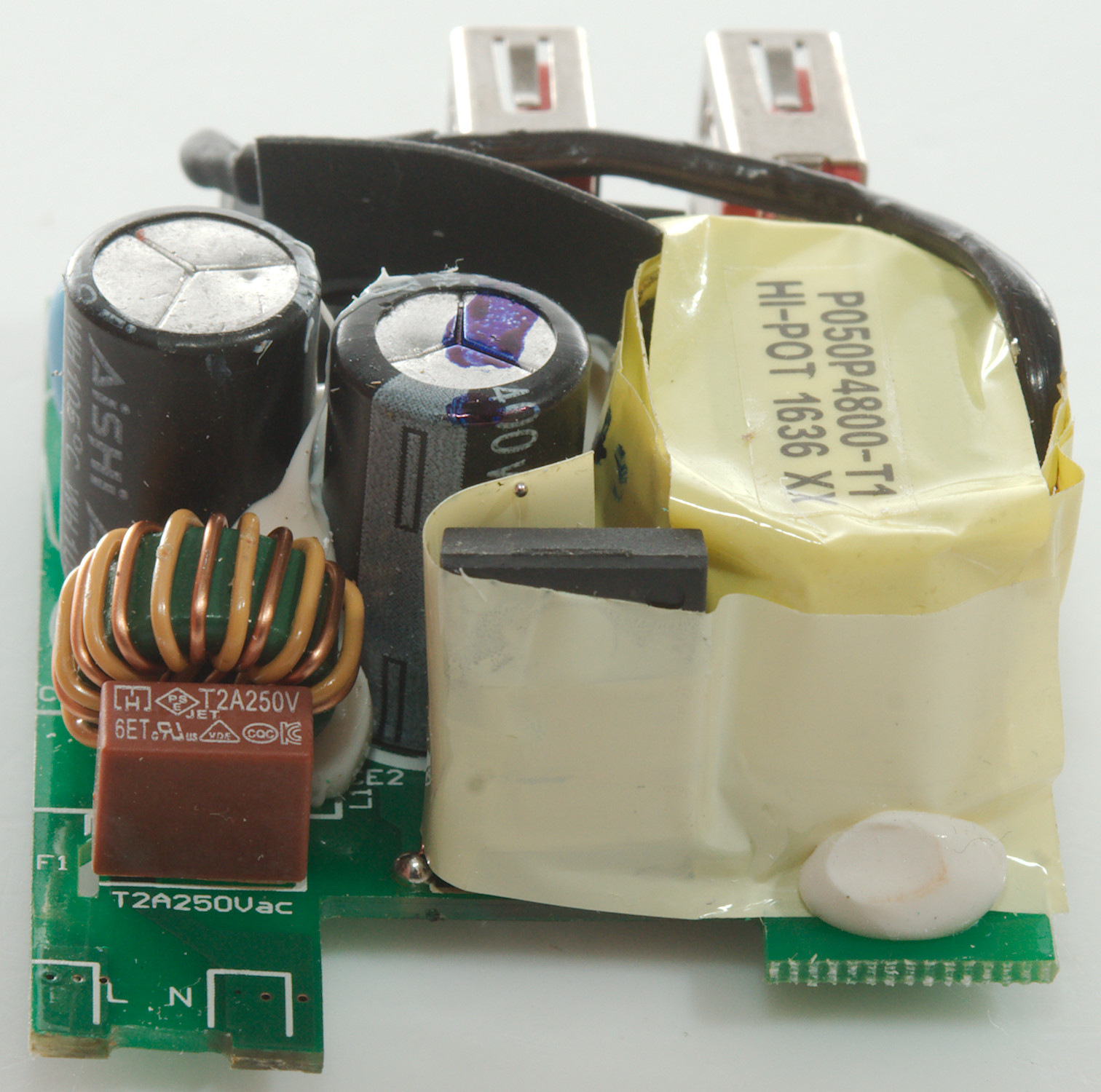
Some pressure with my vice and I could break the bottom off.
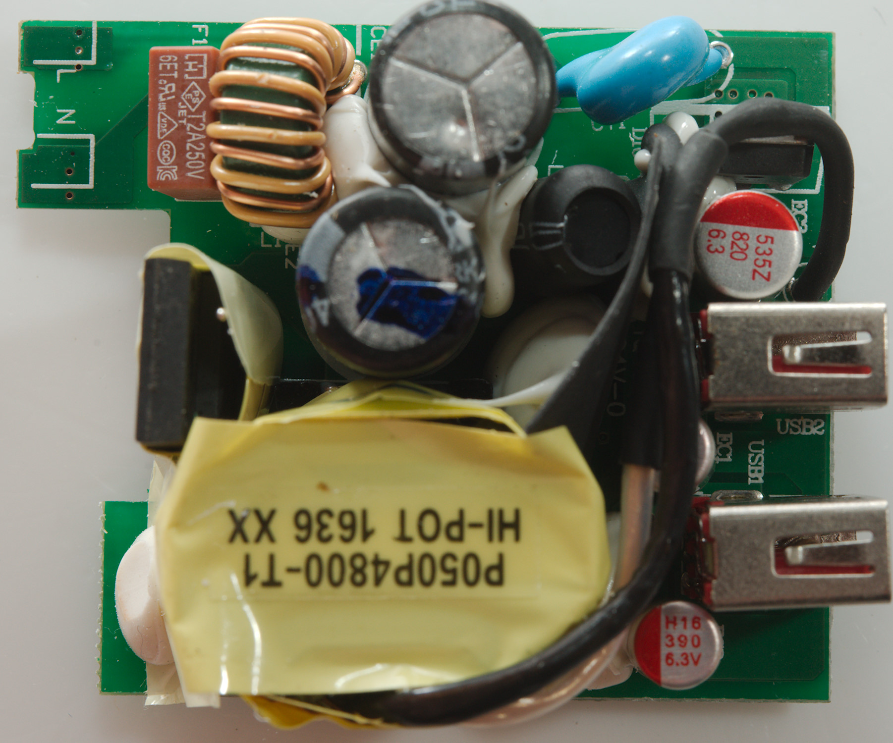
At the mains input is the fuse (F1), then the common mode inductor (L1). There is also two mains smoothing capacitors (CE1 & CE2) with a inductor (L2) between. The mains switcher transistor in next to the transformer and partial hidden in yellow tape.
Between mains and low volt is the usual safety capacitor (CY1). Close to this capacitor is the rectifier transistor (D10) for synchronous rectification.


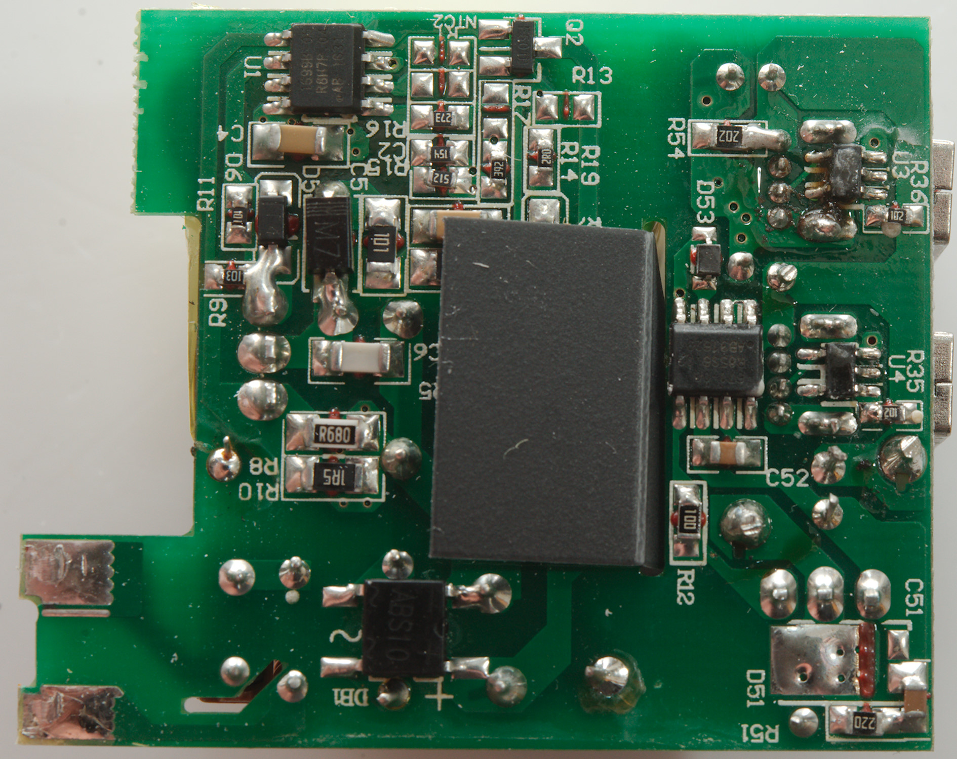
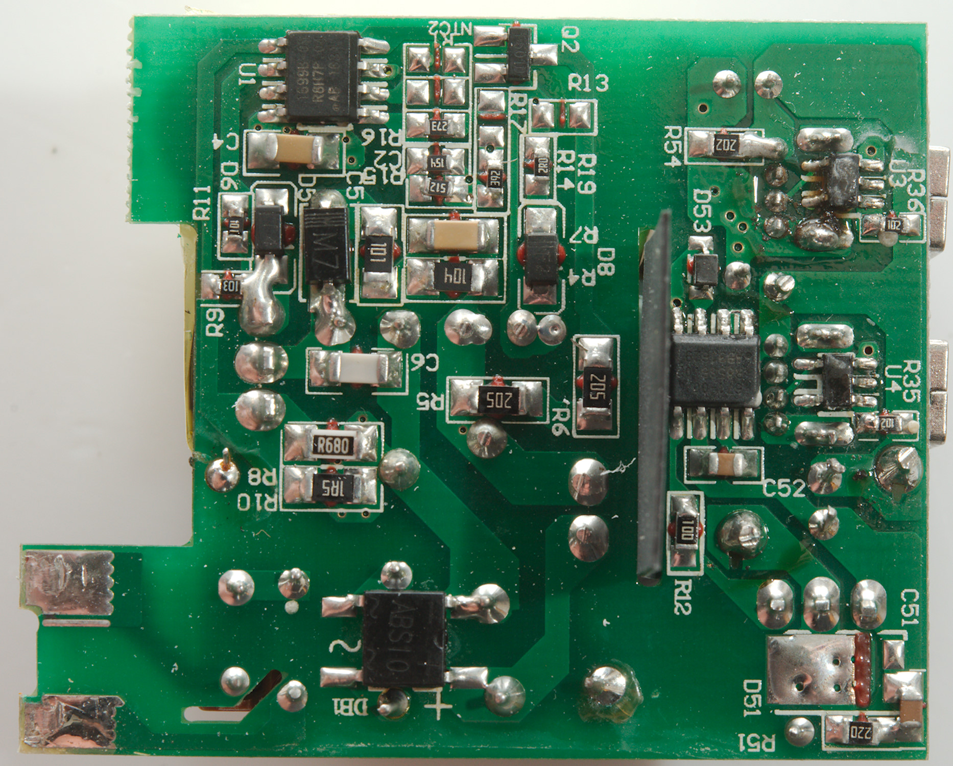
On this side of the board is the rectifier (DB1) and the switcher controller (U1: IW1699), this switcher has a trick with the initial charge circuit: it can be turned off (Q2: FDZ501D N-Channel MOSFET Depletion Mode). This means very low standby/idle current.
On the low volt side is a synchronous rectifier controller (U2: IW671) and two auto code chips (U3 & U4).
Between mains and low volt side is some isolation paper.
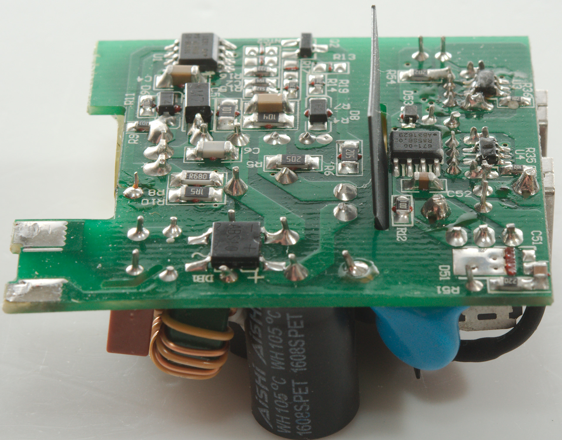
The safety distance is only about 5mm, this is too low for 230V rules, but not directly dangerous.
Testing with 2830 volt and 4242 volt between mains and low volt side, did not show any safety problems.
Conclusion
The charger can deliver the lots of current, but is missing individual port protection, has a good coding and low noise. Safety is slightly low for 230VAC.
Notes
The charger was supplied by a reader for review.
Index of all tested USB power supplies/chargers
Read more about how I test USB power supplies/charger
How does a usb charger work?