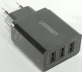
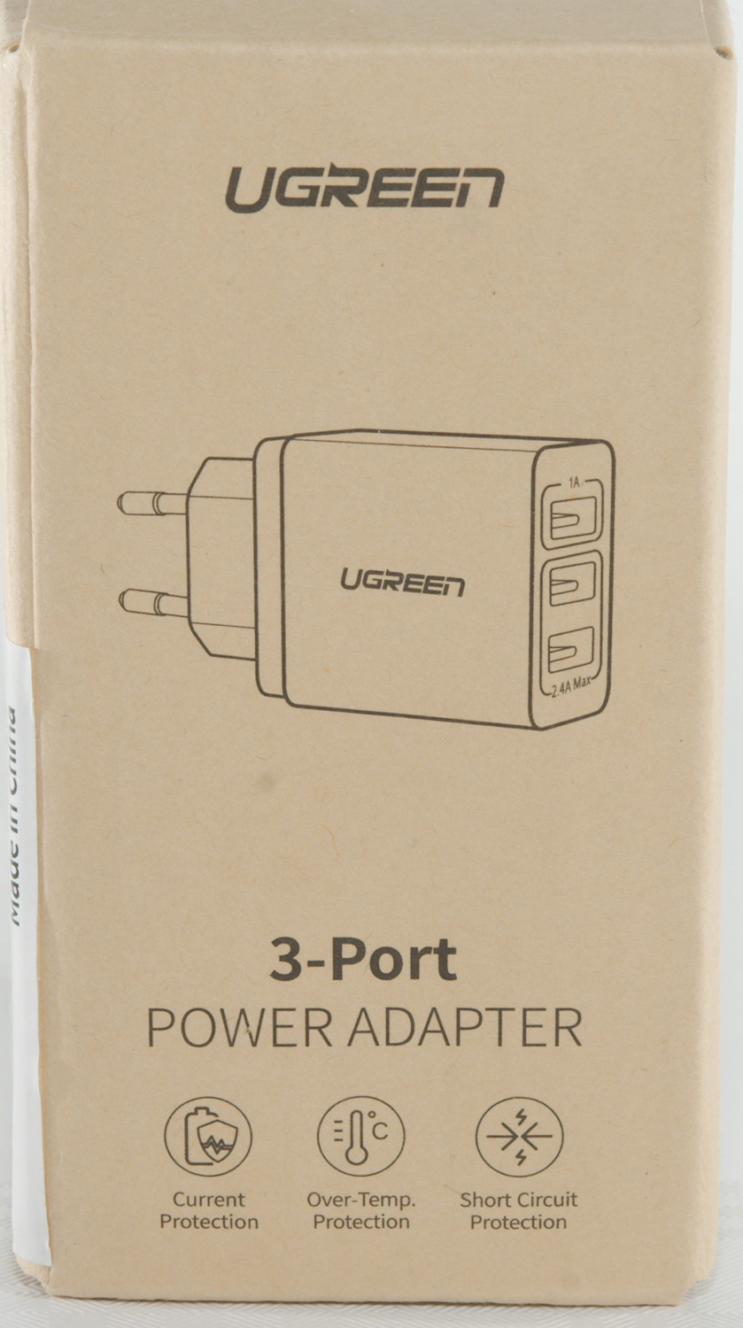
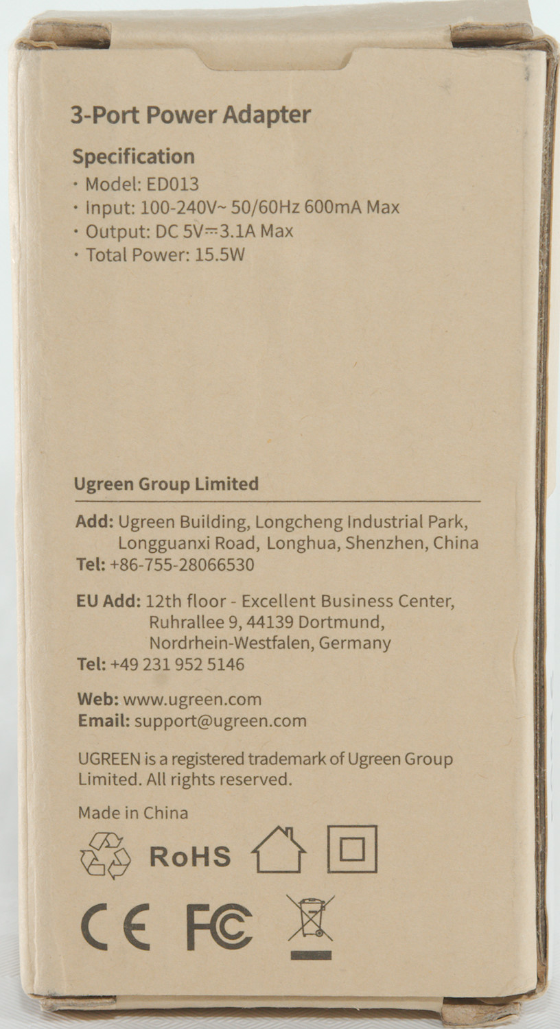
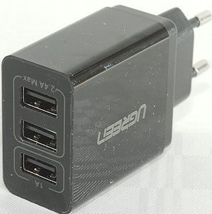
Ugreen 3xUSB 3.1A 15.5W ED013
Official specifications:
-
Total output: 5V3.1A
-
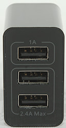
USB 1 Port Current is 5V1A
-
USB 2 and USB 3 Port total current is 5V2.4A Max.
-
If you use USB 2 Port and USB 3 Port at the same time ,single output may be 5V/1.2A Max.
-
If you only use USB2 or USB3 one port, single output current maybe up to 2.4A Max.
I got it from aliexpress dealer: Ugreen Official Store
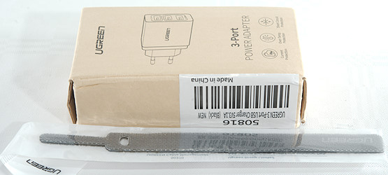
It included a cable strap outside the box.


Measurements
-
Power consumption when idle is 0.06 Watt
-
1A USB output is coded as UB charger (DCP)
-
Top 2A USB output is coded as Apple 2.4A, DCP, QC 5V
-
Bottom 2A USB output is coded as Apple 2.4A
-
USB outputs are in parallel
-
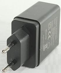
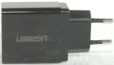
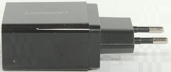
Weight: 59.4g
-
Size: 88.3 x 45.5 x 26.7mm

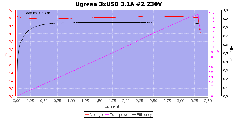
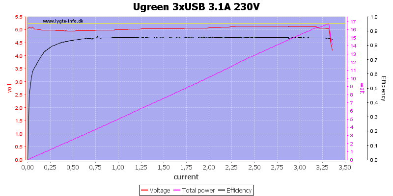
The USB output has overload protection at about 3.3A, this fits nicely with the total rating for the charger, but not with the ports 1A rating. The charger has cable compensation.

It is not really any surprise that the two other ports looks the same.
This also means that the curve is the same with all ports in parallel.
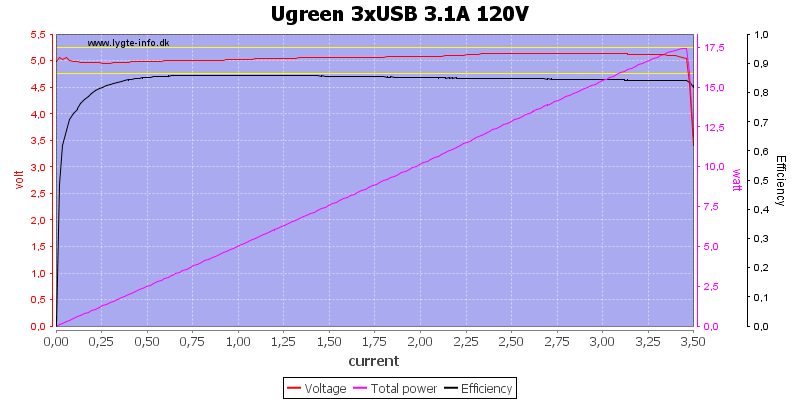
At 120VAC the output current is slightly higher.
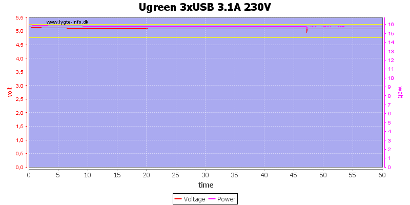
For a load test I used 3.1A load for one hour, it worked fine.
The temperature photos below are taken between 30 minutes and 60 minutes into the one hour test.
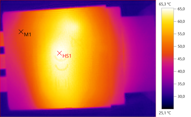
M1: 47.7°C, HS1: 65.3°C
HS1 is the transformer an the other hot spot is the synchronous rectifier.
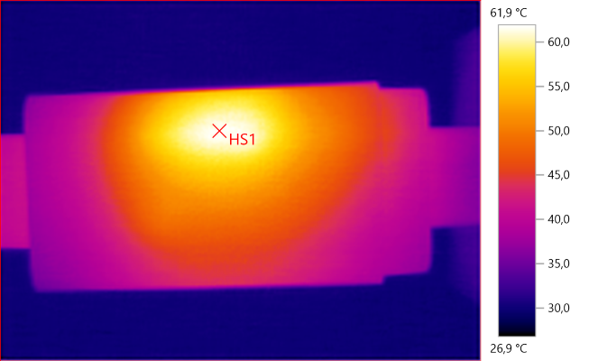
HS1: 61.9°C
Here HS1 is due to the switcher IC.
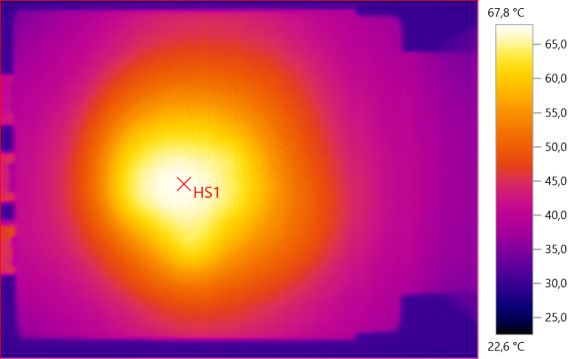
HS1: 67.8°C
The transformer is heating the enclosure.
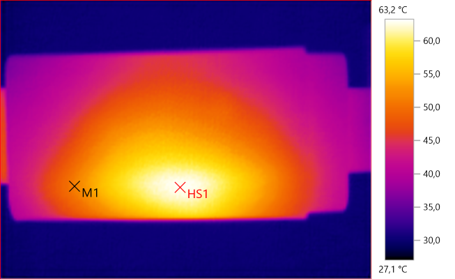
M1: 51.1°C, HS1: 63.2°C
Here HS1 is the synchronous rectifier.
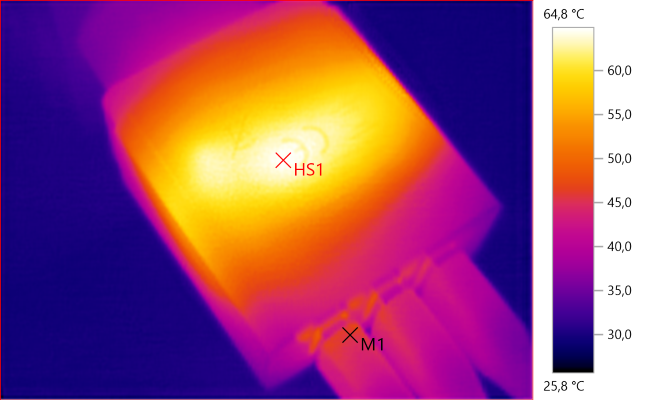
M1: 45.9°C, HS1: 64.8°C
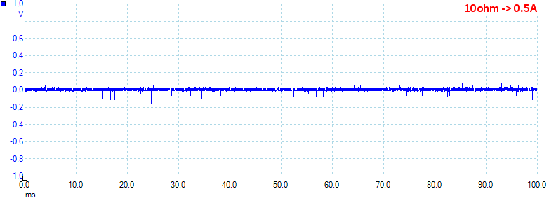
At 0.5A the noise is 8mV rms and 157mVpp.
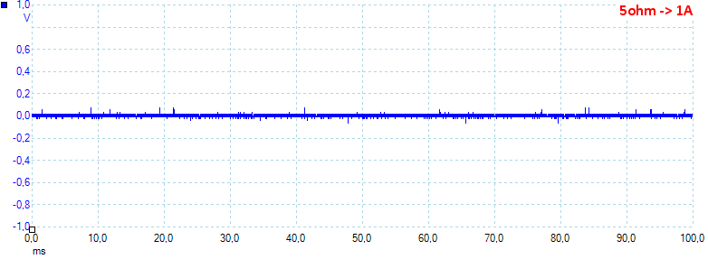
At 1A the noise is 15mV rms and 268mVpp.
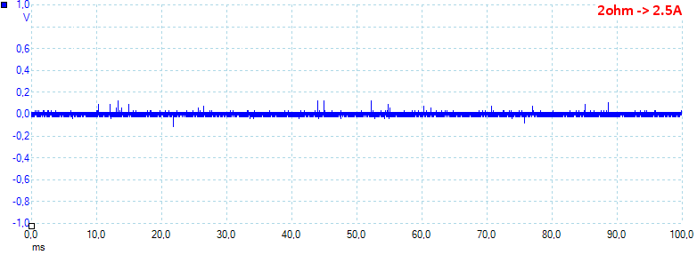
At 2.5A the noise is 18mV rms and 331mVpp, this is low noise.
Tear down
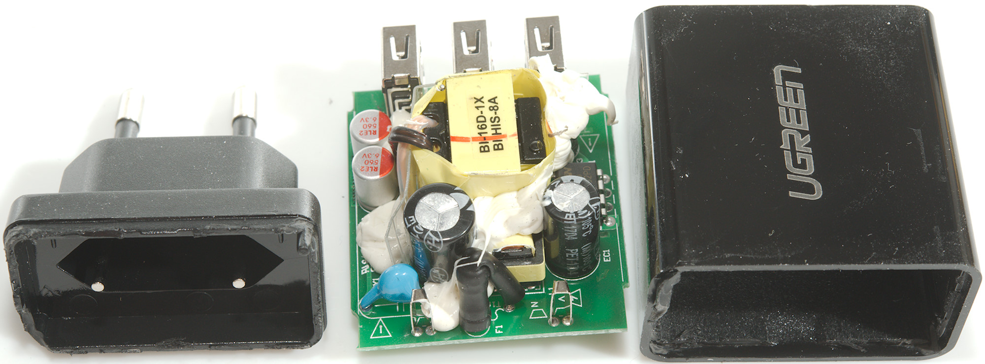
Using my vice to crack the glue, then whacking it with a mallet got it open.

At the mains input the fuse (F1) is hidden in shrink wrap, there is a common mode coil (L1) between the mains smoothing capacitors (EC1 & ?). There is a safety capacitor (CY1) to the low volt side. The mains switcher is on the other side of the transformer (U1: PN8386: 18W).
There is some clear plastic between mains and low volt side for better protection.

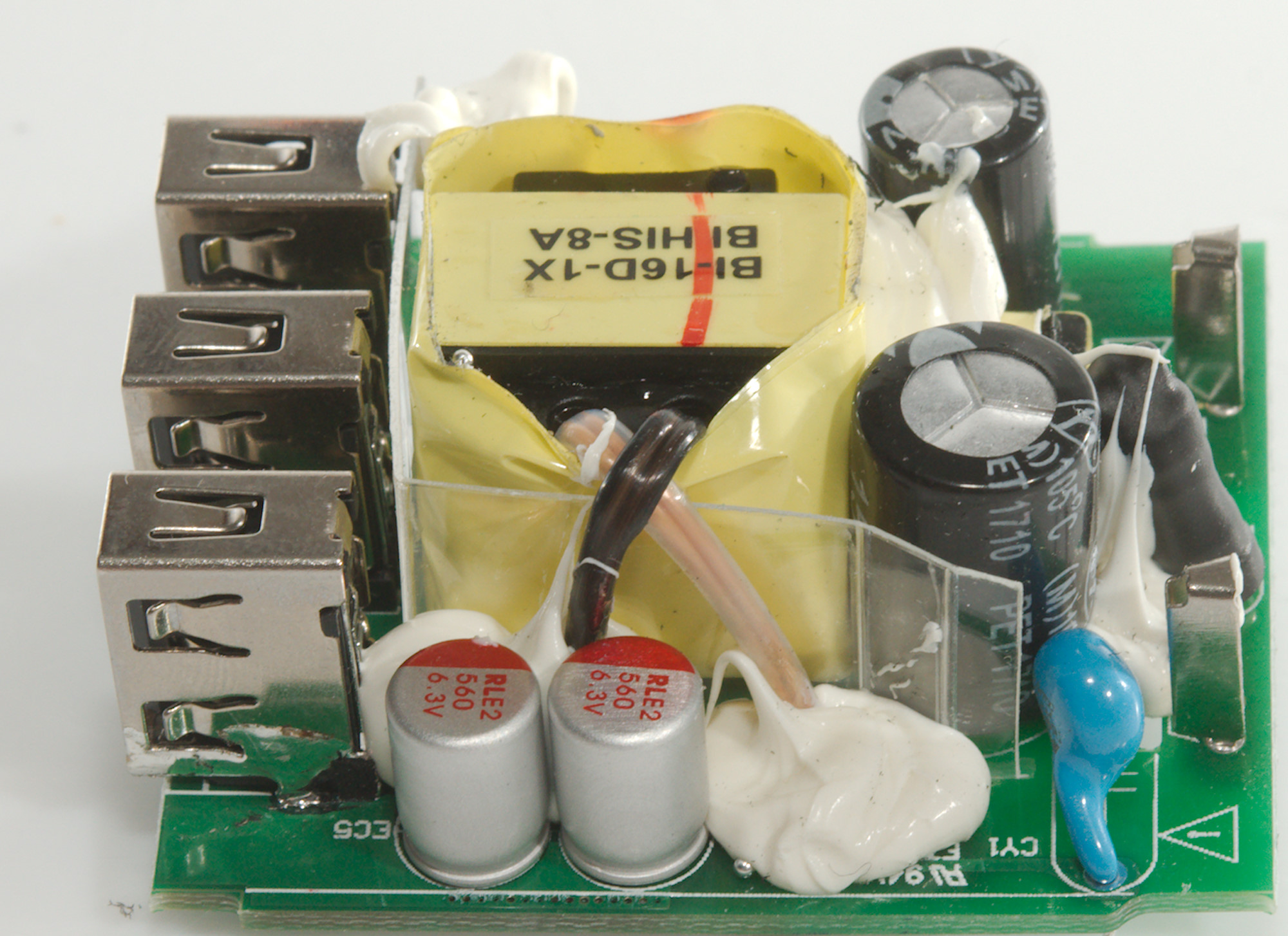
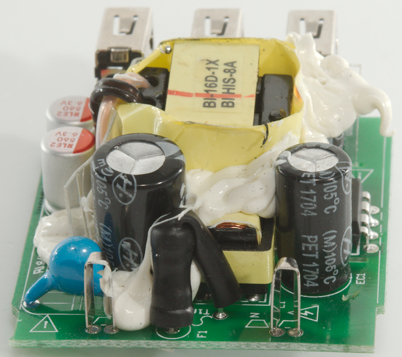
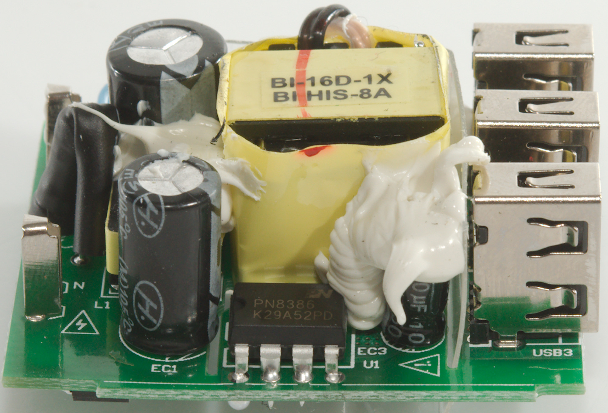
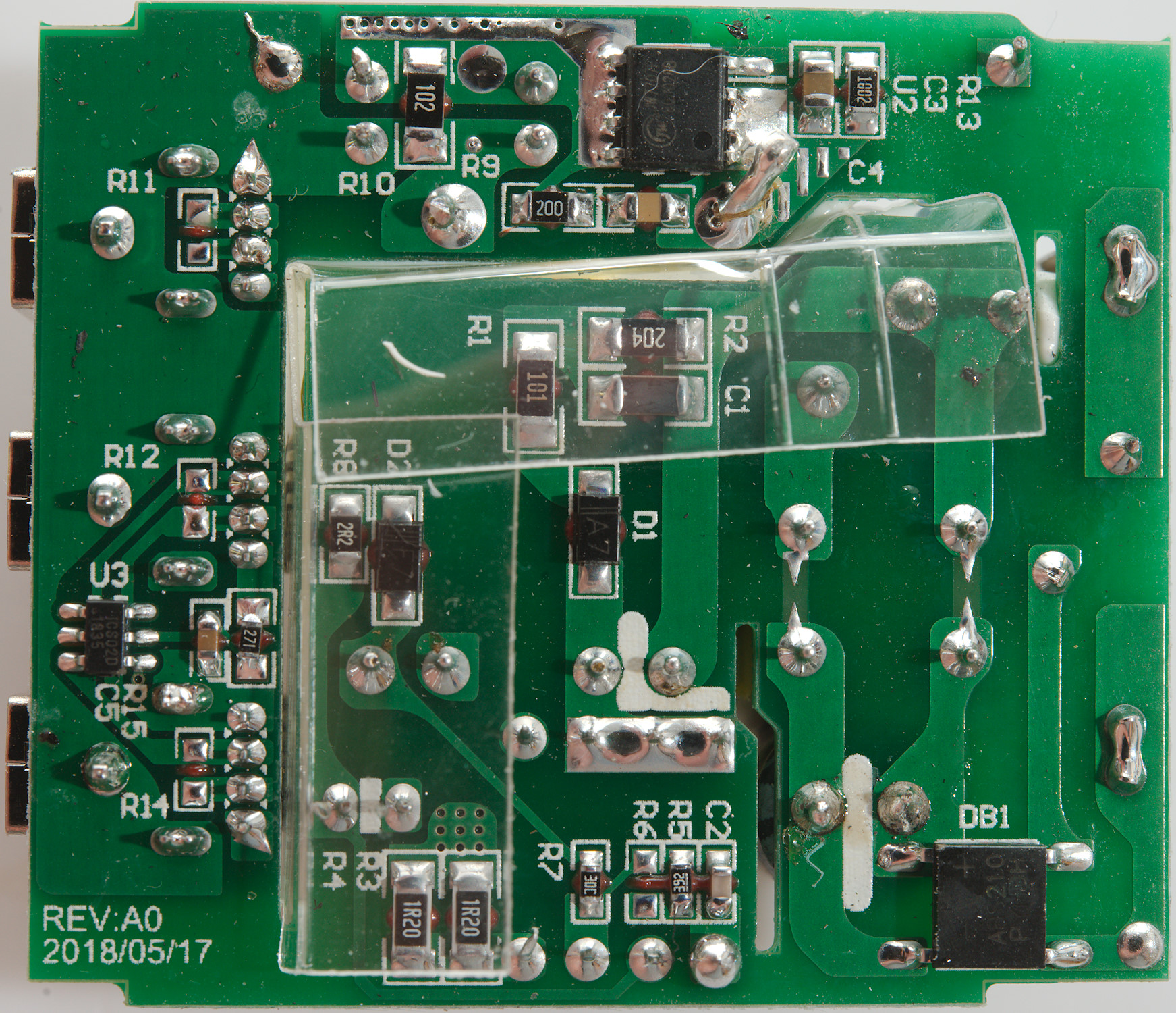
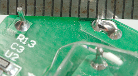
On this side is the bridge rectifier (DB1), the synchronous rectifier chip (U2: JW7707F: 50V 7mOhm). There is a coding chip (U3: Marked ICS03D) to some of the USB connectors, but I did not see any automatic coding on the USB connectors.
The clear plastic goes through slots in the circuit board and also increases safety on this side.
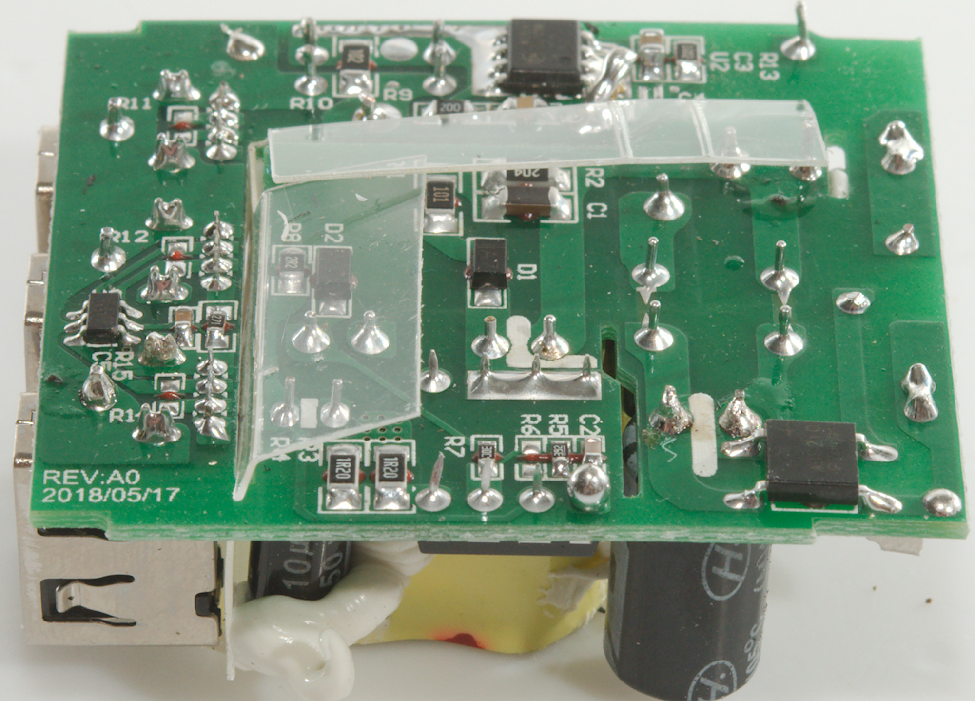
Even with all the plastic the final device is a bit low on distance between mains and low volt side, it is only about 5mm and not above 6mm.
Testing with 2830 volt and 4242 volt between mains and low volt side, did not show any safety problems.
Conclusion
This USB charger is a bit weak for a 3 port charger and is missing a good auto coding, but it works fine with good protection. The safety is slightly low due to the too short distance, but it is not a serious problem.
Notes
Index of all tested USB power supplies/chargers
Read more about how I test USB power supplies/charger
How does a usb charger work?
