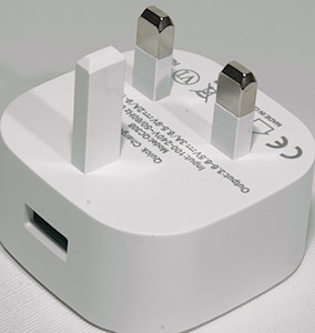
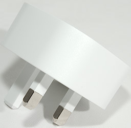
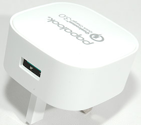
Papalook QC3 charger QC308
Official specifications:
-
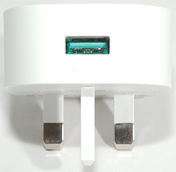
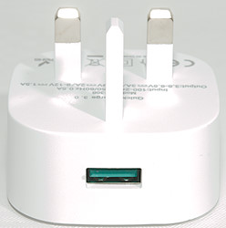
Port: Single USB charging port
-
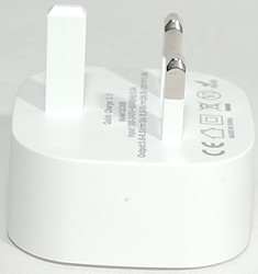
input: AC100-240V~50/60Hz 0.5A
-
Output: 3.6-6.5V 3A / 6.5-9V 2A / 9-12V 1.5A
-
Size: 52 x 52 x 24mm
I got it from ebay dealer: papalook_official_us
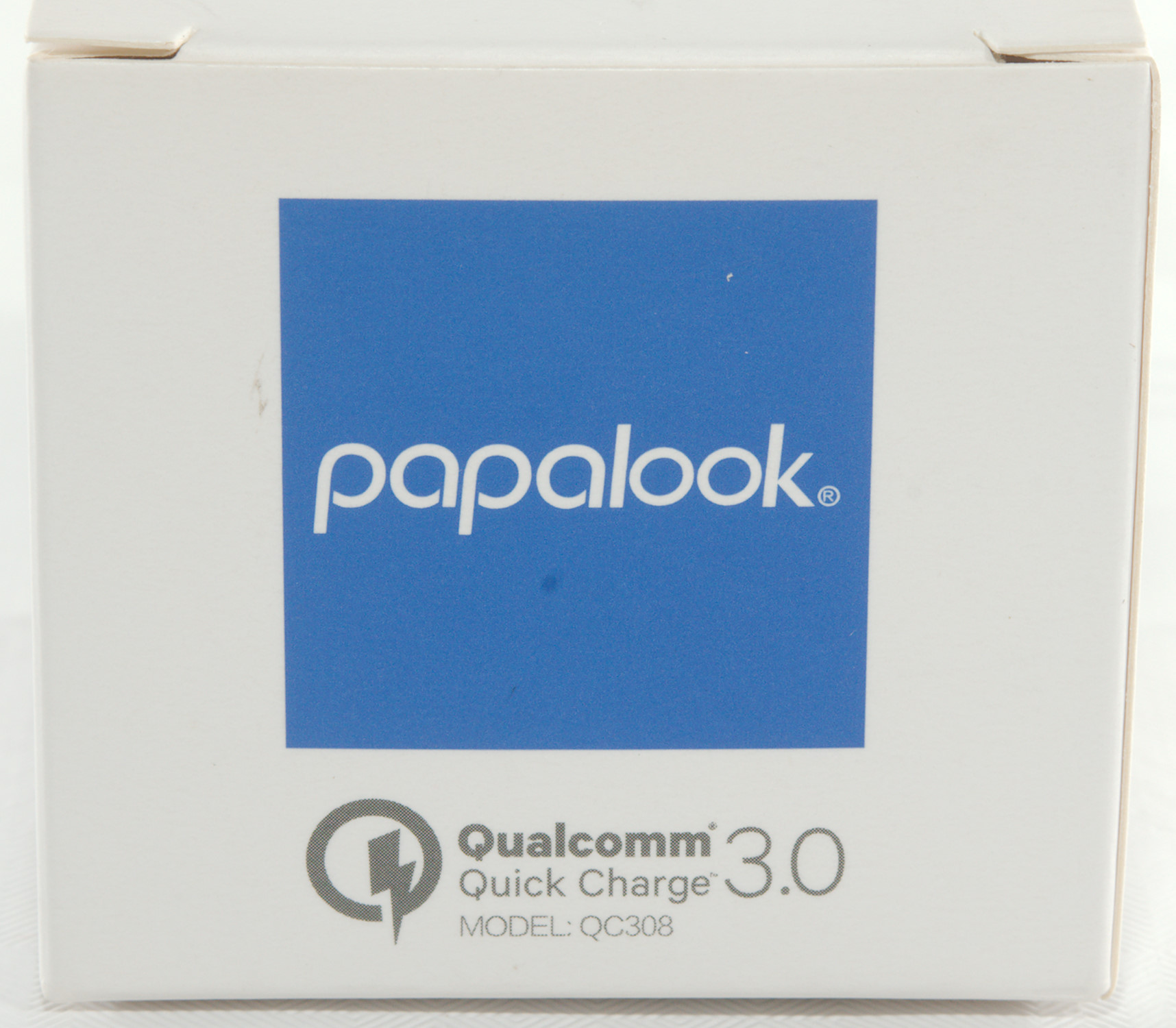

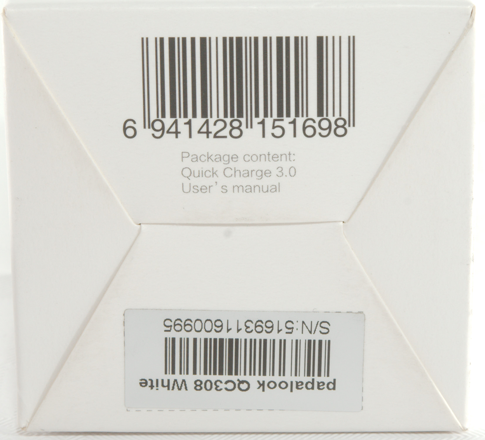

The charger arrived in a white cardboard box.
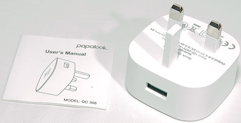
It contained the charger and a instruction sheet.

Measurements
-
Power consumption when idle is 0.05 Watt
-
Minimum QC3 voltage: 4.3V
-
USB output is coded as DCP and QC3
-
Weight: 59.5g
-
Size: 51.7 x 51.7 x 47.0mm
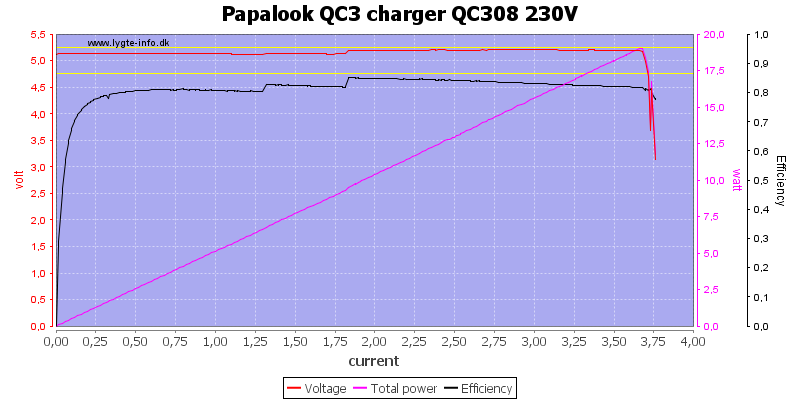
The charger is rated for 3A and can deliver about 3.7A on 5V, this is acceptable. There is some cable compensation.
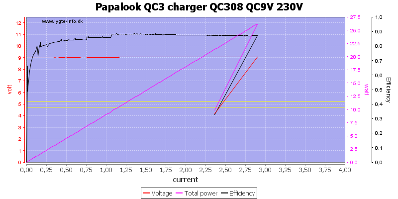
At 9V the current is down to 2.8A, it is well above the rated 2A
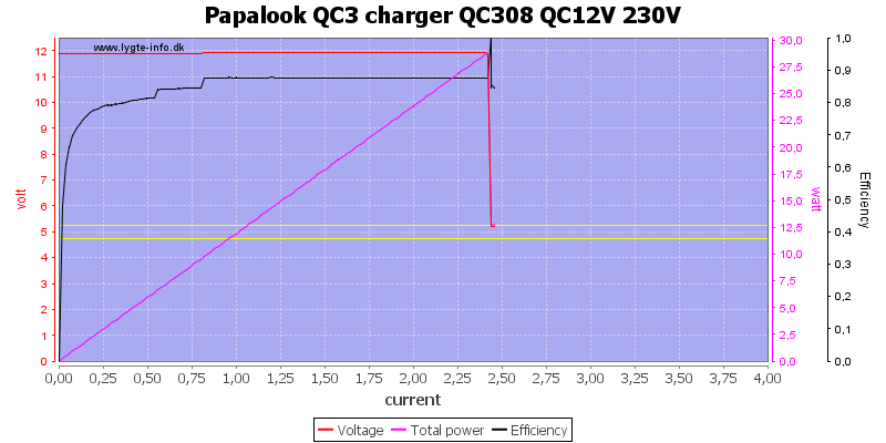
At 12V the current is about 2.4A, again well above the 1.5A rating.
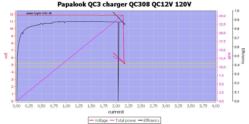
With 120VAC input the current is “only” 2.1A.
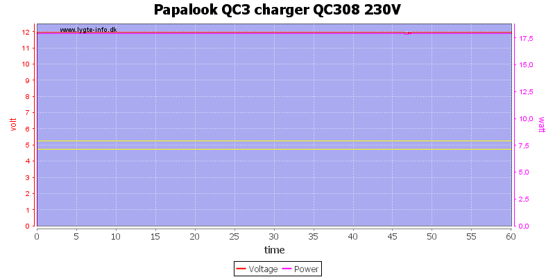
For a load test I used 12V 1.5A load for one hour, it worked fine.
The temperature photos below are taken between 30 minutes and 60 minutes into the one hour test.
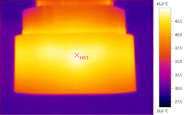
HS1: 45.0°C
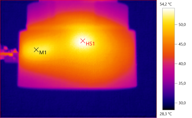
M1: 51.5°C, HS1: 54.2°C
HS1 must be from the heatsink pins on the large chip. M1 is the white stuff transferring heat from the circuit board to the enclosure.
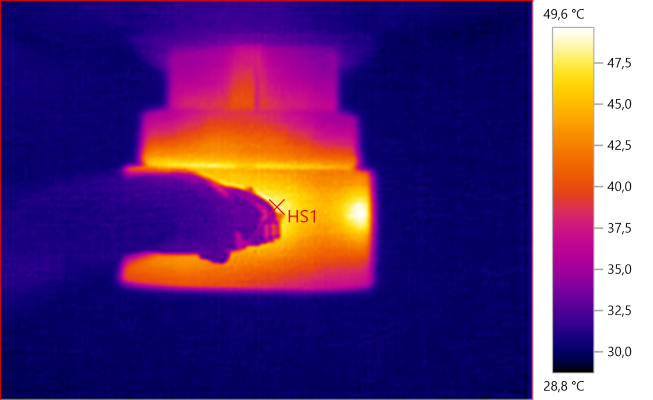
HS1: 49.6°C
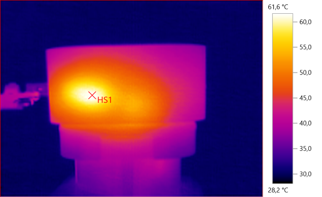
HS1: 61.6°C
HS1 is the synchronous rectifier transistor transferred through the white stuff.
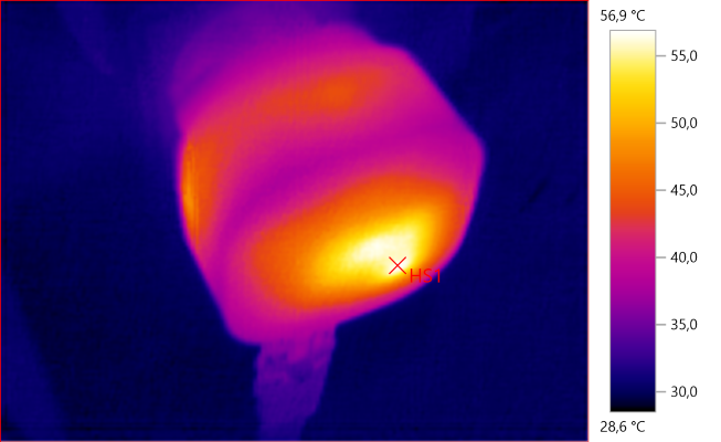
HS1: 56.9°C
HS1 is the transformer.
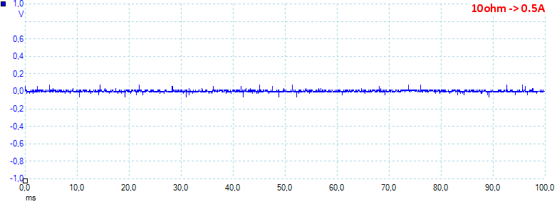
At 0.5A the noise is 8mV rms and 170mVpp.
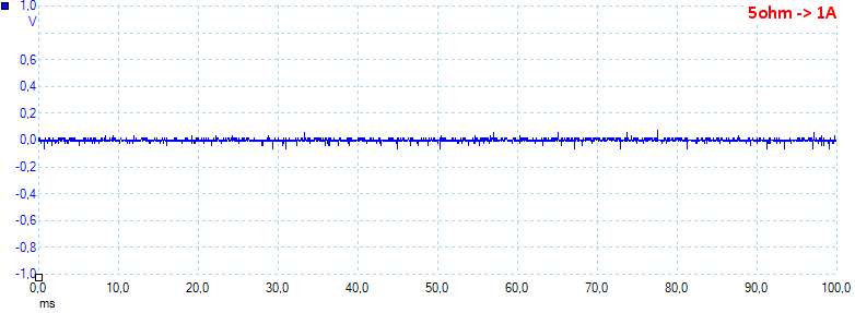
At 1A the noise is 20mV rms and 172mVpp.
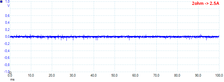
At 2.5A the noise is 17mV rms and 213mVpp.
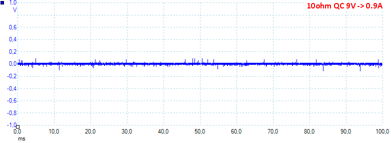
At 9V 0.9A the noise is 10mV rms and 184mVpp.
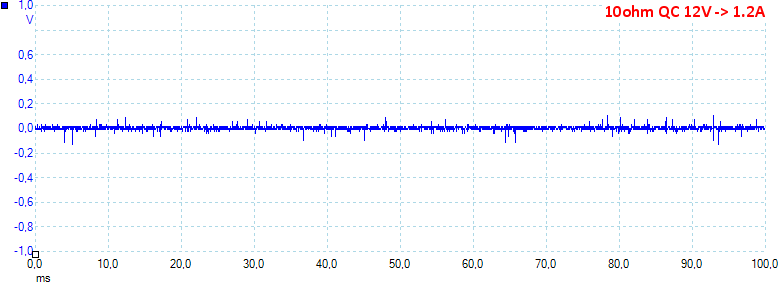
At 12V 1.2A the noise is 14mV rms and 262mVpp.
Tear down

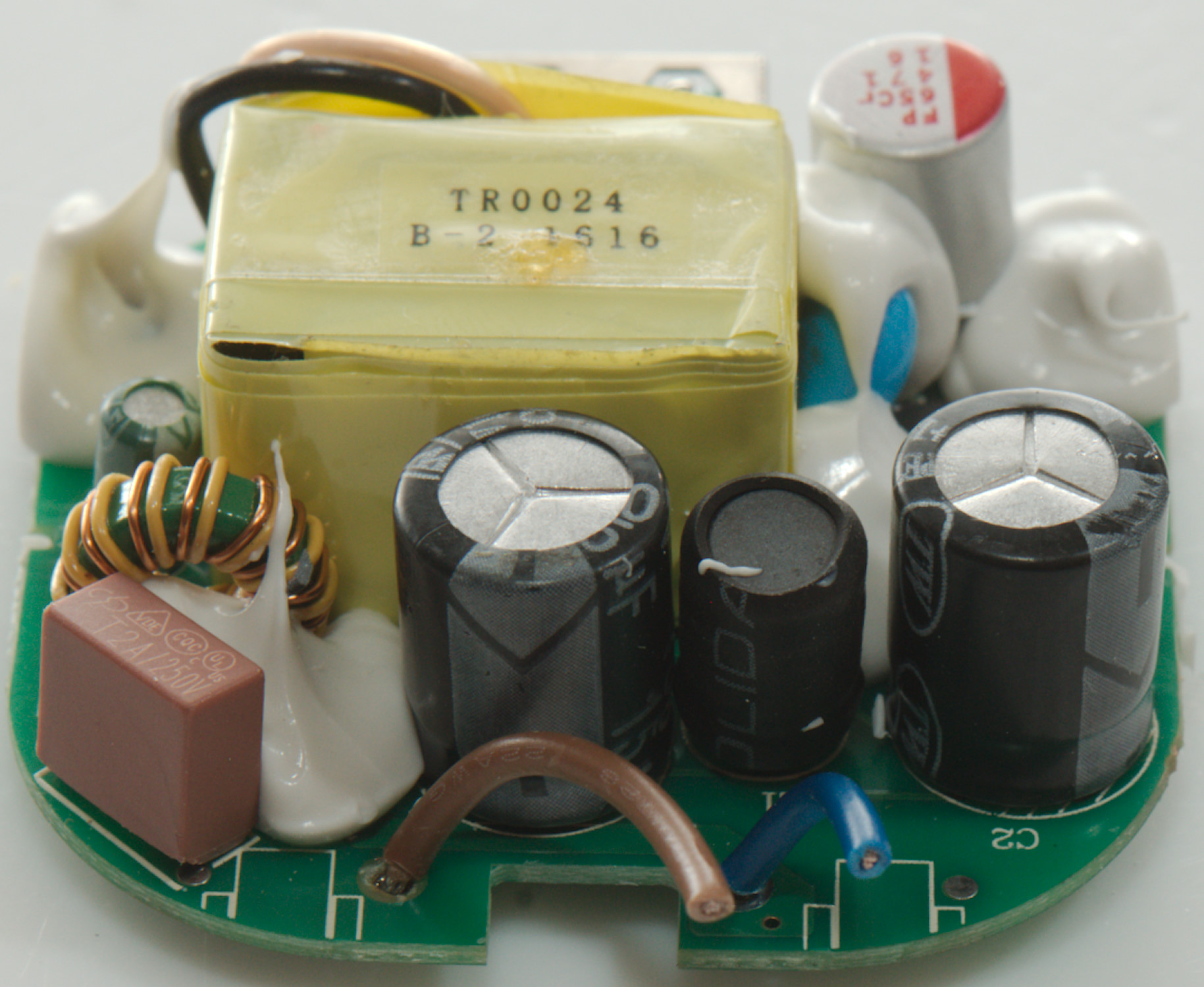
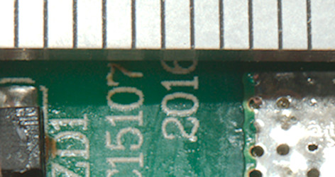
I could not pop the lid on this charger and had to cut a bit. The circuit board is glued in.
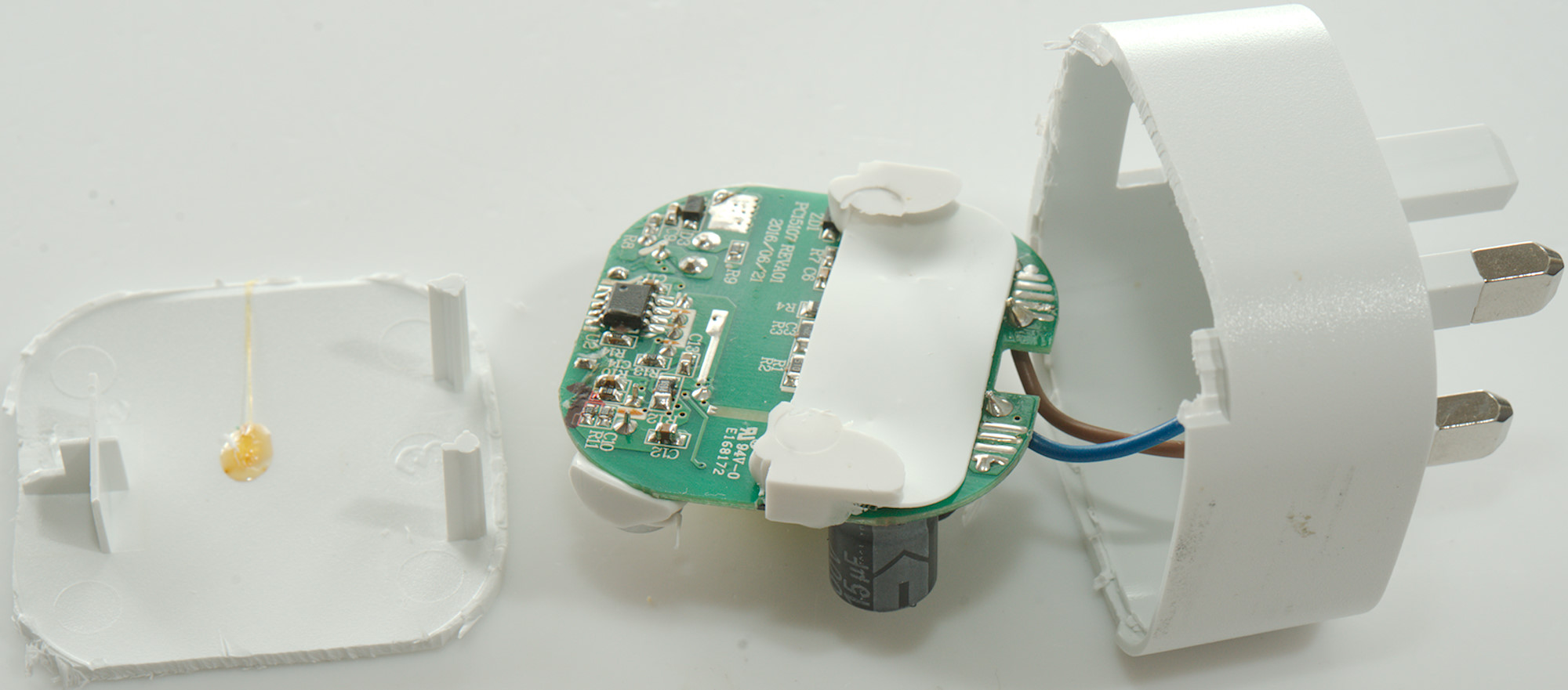
There is also some support on the led and isolation between the mains terminals and the charger circuit board.
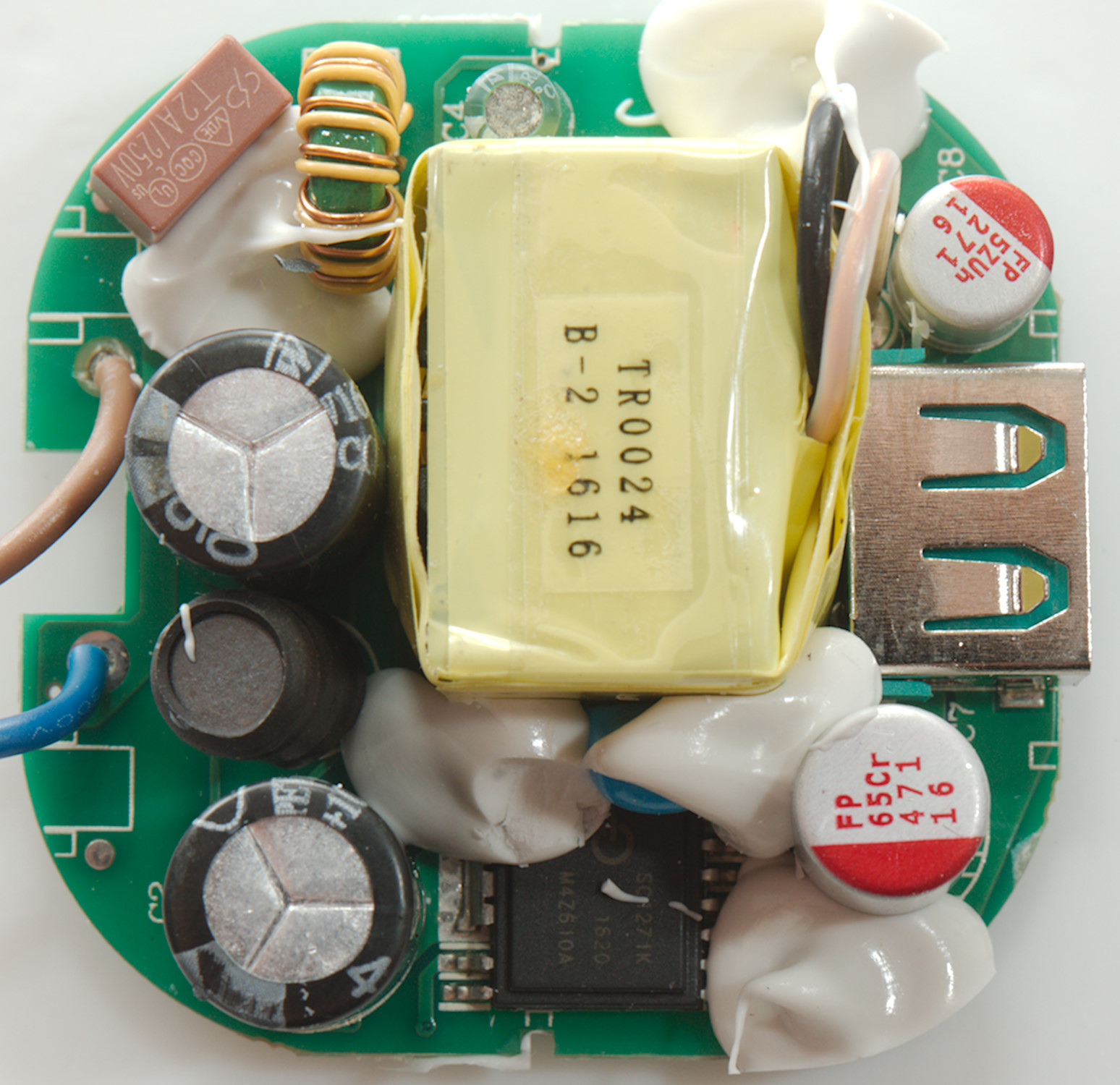
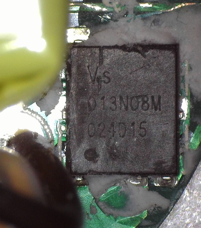
There is a fuse and a common mode coil at the input. The two smoothing capacitors has a inductor between them. All the electronic is basically in one IC (SC1271K). It looks like the soldering of the wide terminal on the IC could be better (This is for heatsinking).
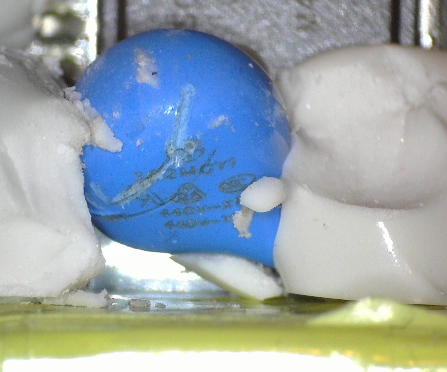
Hidden beneath the white stuff is a rectifier transistor for the synchronous rectifier. The safety capacitor looks fine (The crack is from my screwdriver when breaking it out).

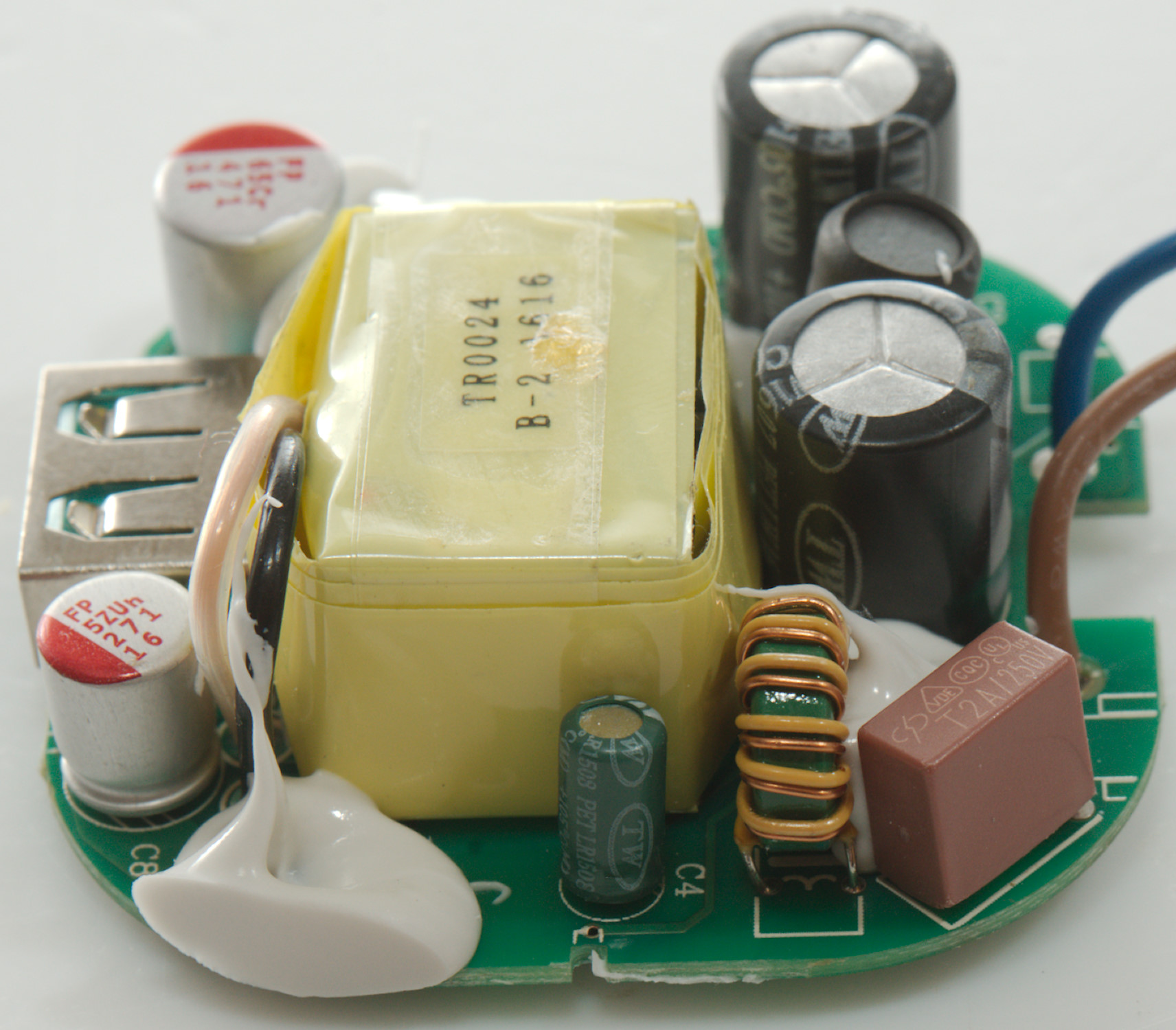
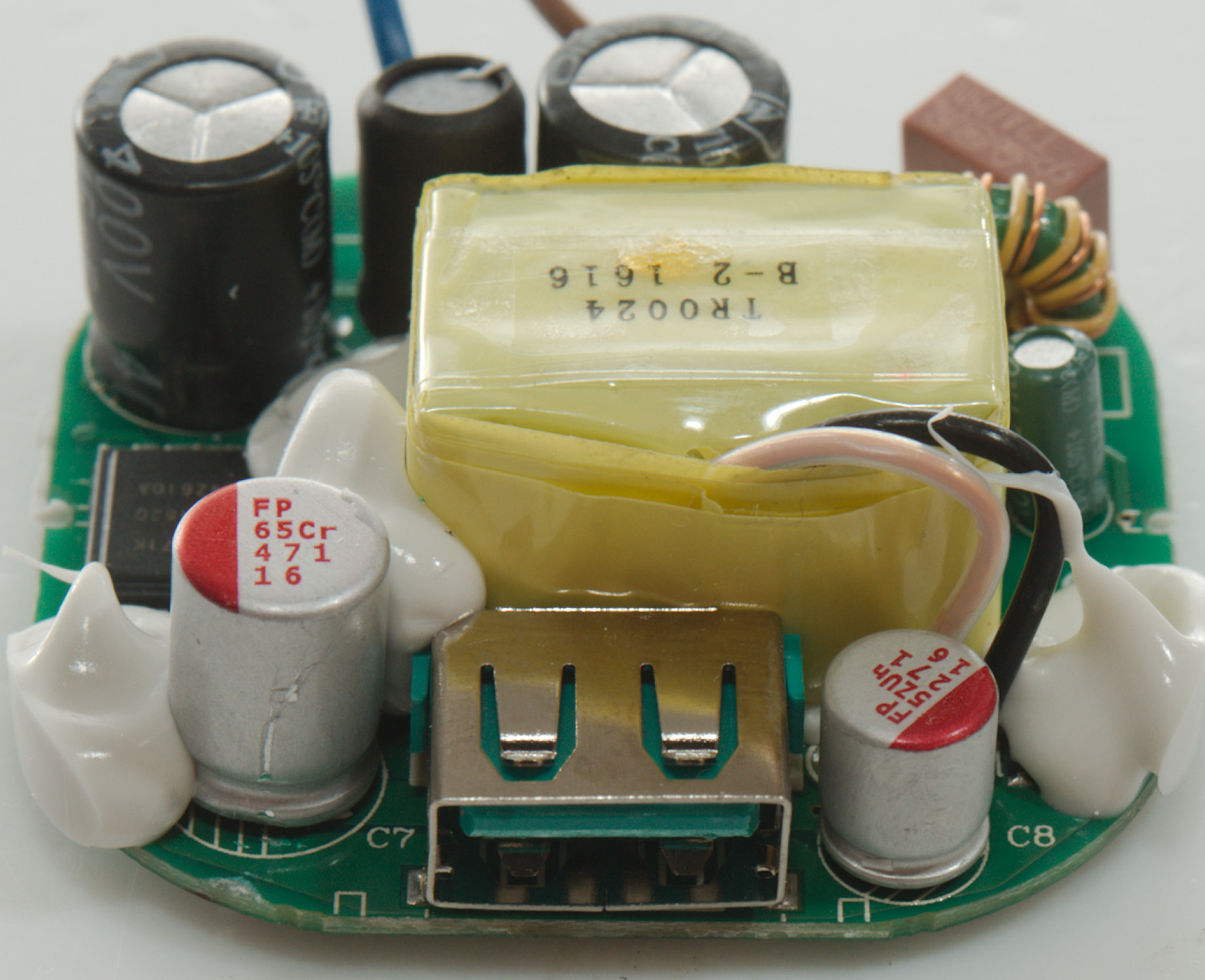
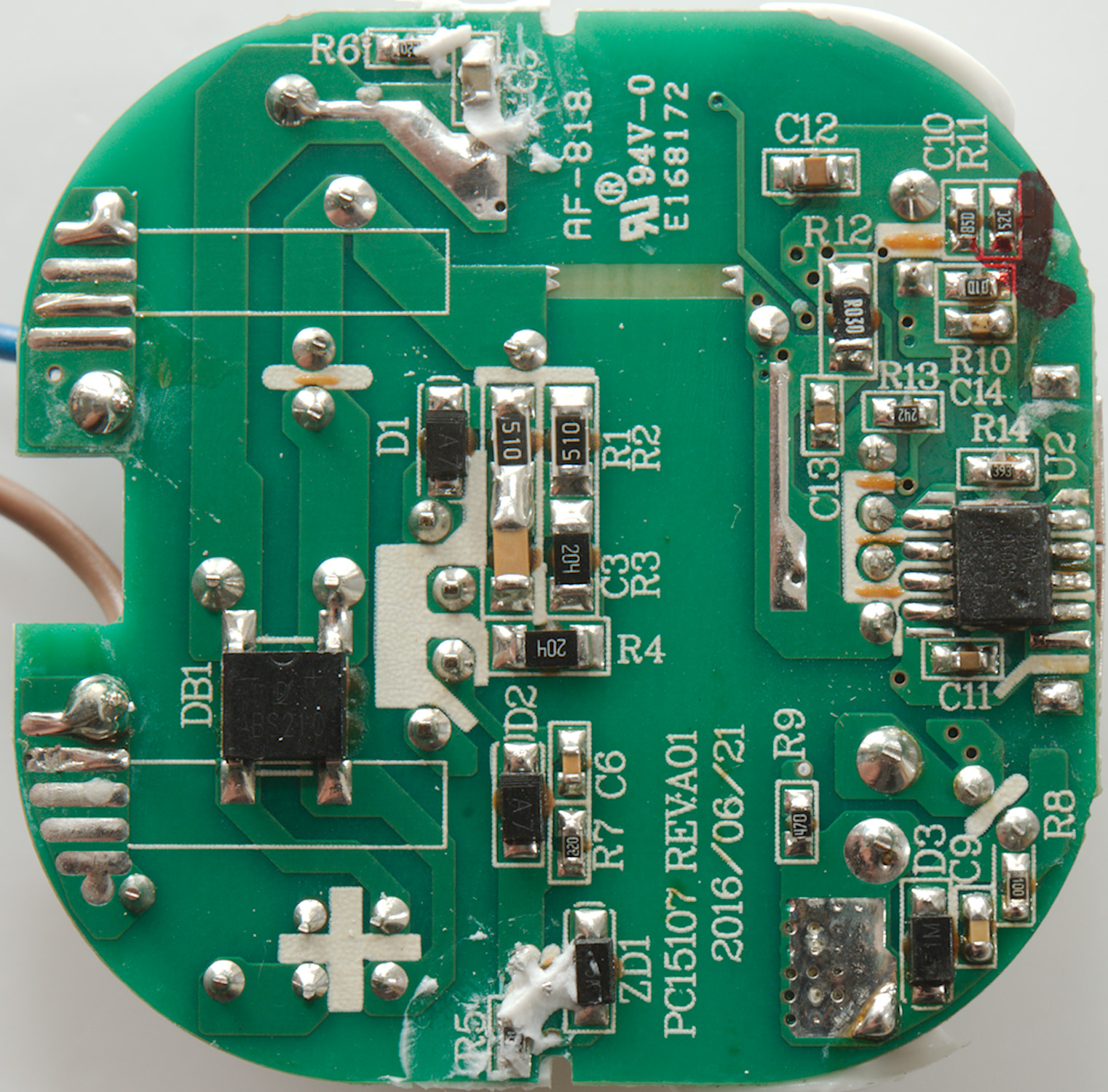
Saying all the electronic is in the big chip is not completely correct, the bridge rectifier is here together with some resistors and capacitors.
There is also the QC controller
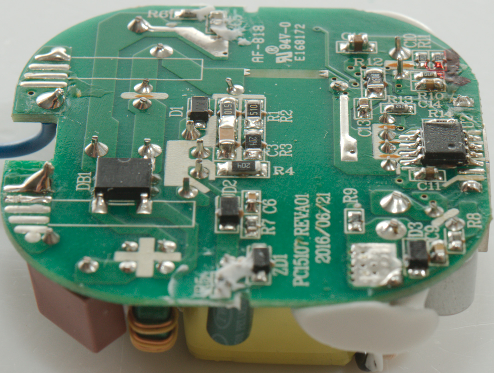
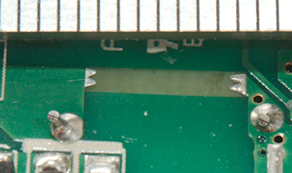
The distance between mains and low volt side good.
Testing with 2830 volt and 4242 volt between mains and low volt side, did not show any safety problems.
Conclusion
The charger can easily deliver rated current, the temperature increase is moderate, the noise is low, safety looks fine, but it only supports DCP and QC. This may be enough, but is not as universal as some other chargers with more high voltage protocols.
All in all it looks like a good charger.
Notes
The charger was supplied by a reader for review.
Index of all tested USB power supplies/chargers
Read more about how I test USB power supplies/charger
How does a usb charger work?