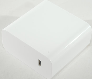
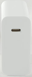
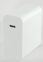
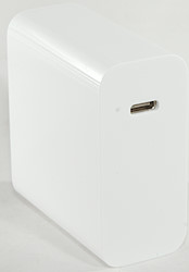
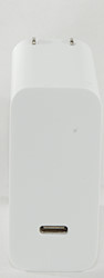
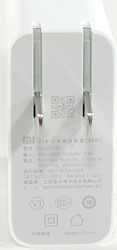
Xiaomi Mi 65W USB-C charger CDQ07ZM
Official specifications:
-
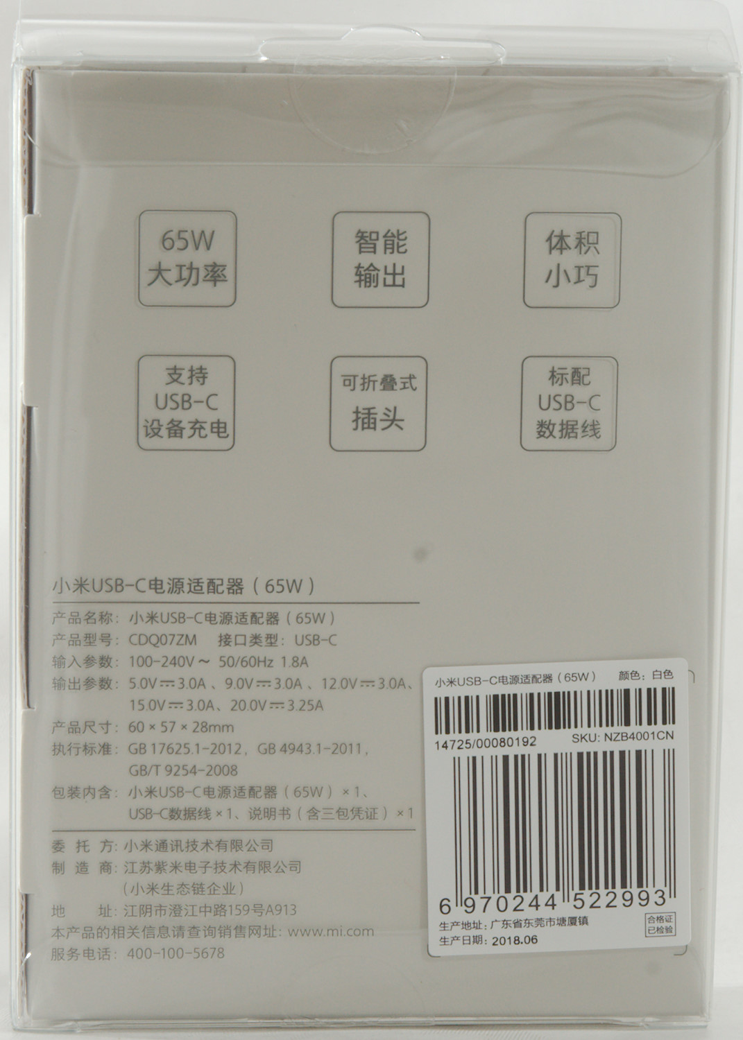
Name: xiaomi USB-C charger 65W
-
Model number: CDQ07ZM
-
port: USB-C
-
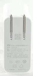
Input: 100-240V - 50/60HZ 1.8A
-
Output: 5.0V- 3.0A / 9.0V- 3.0A / 12.0V- 3.0A / 15.0V- 3.0A / 20.0V- 3.25A
-
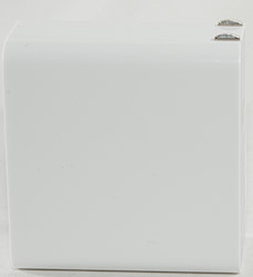
Size: 60*57*28mm
I got it from aliexpress dealer: Dtop Store
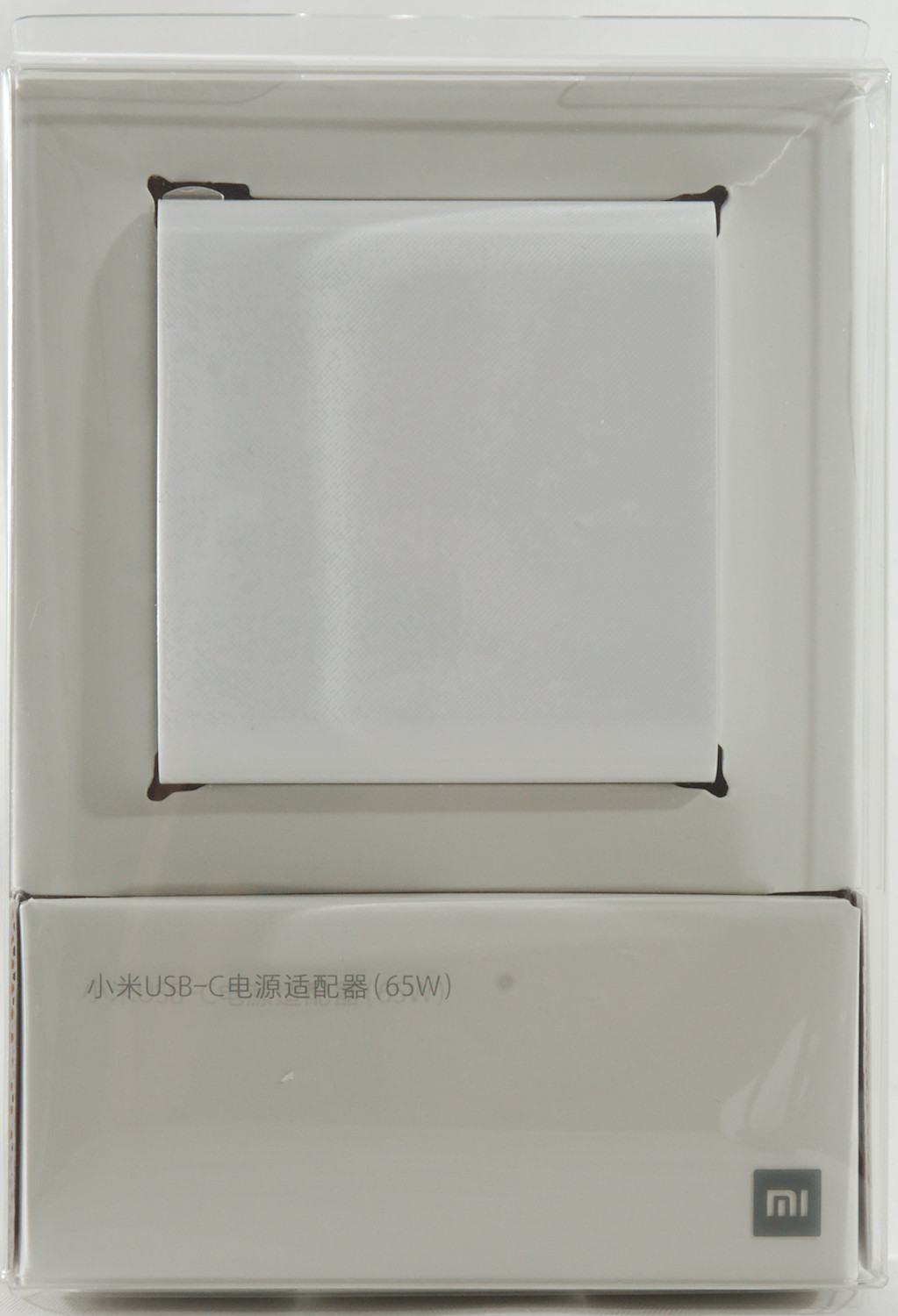
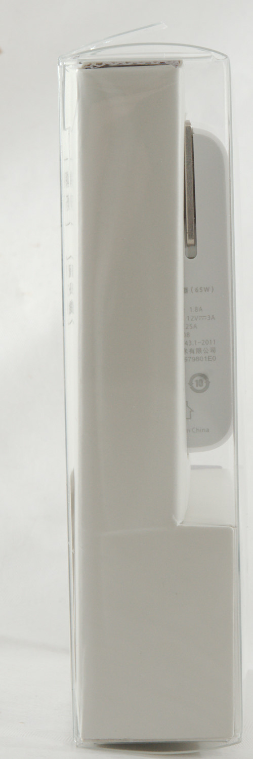

I got it in a cardboard box with specifications on the back.
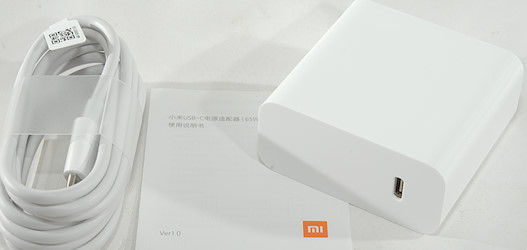
The box contained the charger, a usb cable and a instruction sheet in Chinese
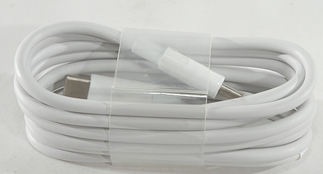
The supplied cable can handle 3.25A with USB-C
Measurements
-
Power consumption when idle is 0.08 watt
-
PD output supports: 5V 3A, 9V 3A, 12V 3A, 15V 3A, 20V 3A, 20V 3.25A
-
PD output also support DCP and QC3
-
Default PD output is off.
-
Weight: 115g
-
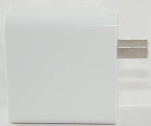
Size: 61.3 x 57 x 28mm with legs folded
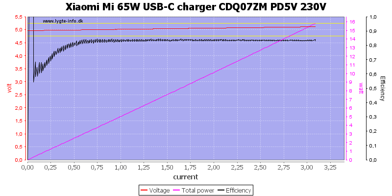
At 5V the overload protection is at about 3.1A, this is very good for a 3A rating.
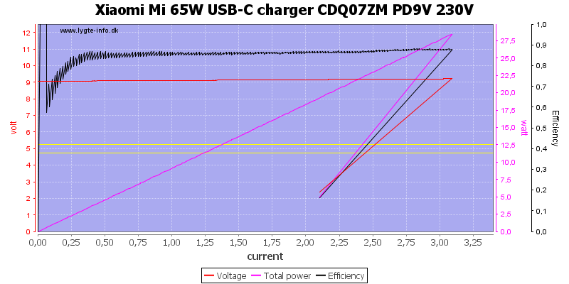
It is the same at 9V
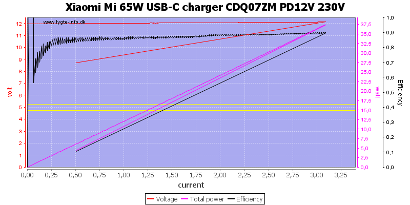
And 12V
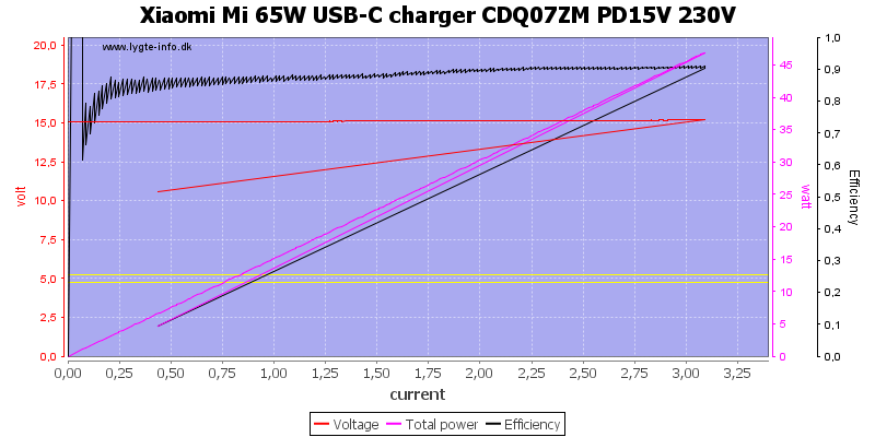
15V is also 3.1A
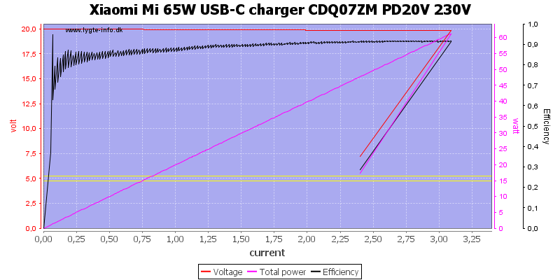
And 20V is also 3.1A. Oops something is wrong, the charger is rated for 3.25A at this voltage. The reason is the cable, it is raporting 3A as max current.
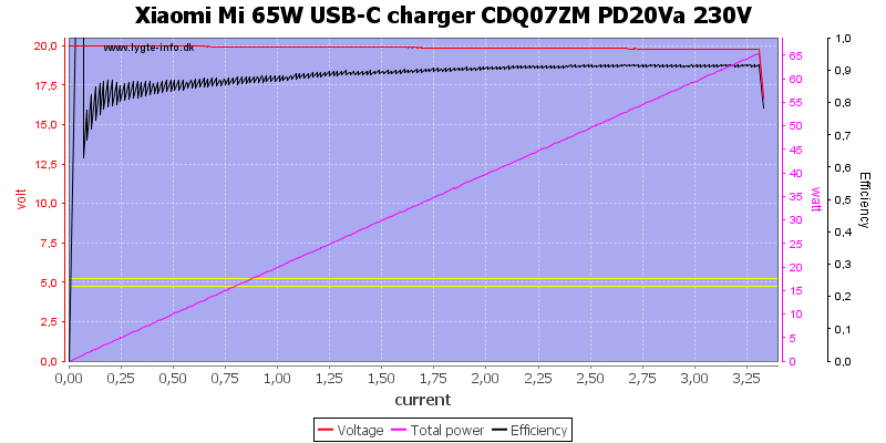
With a 5A cable the current limit is moved to about 3.3A. I was a bit impressed that it not only change the electronic report, but also change current limit depending on cable.
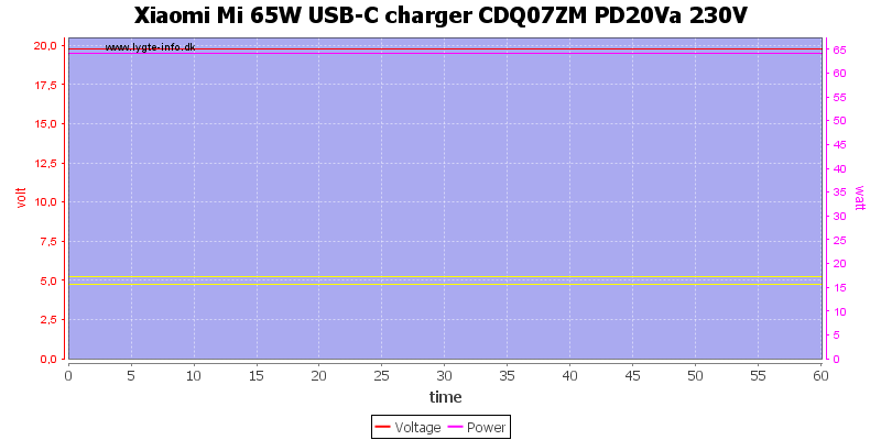
For a load test I used 20V 3.25A for one hour, it worked fine.
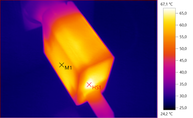
The temperature photos below are taken between 30 minutes and 60 minutes into the one hour test.
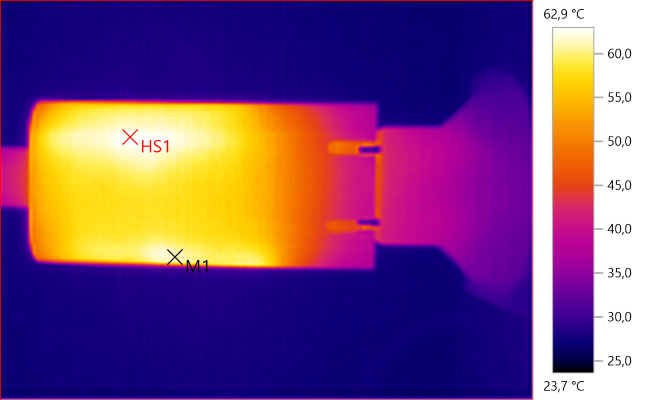
M1: 61.3°C, HS1: 62.9°C
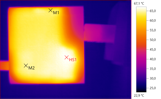
M1: 62.7°C, M2: 64.4°C, HS1: 67.1°C
HS1 is the transformer.
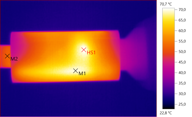
M1: 69.6°C, M2: 52.0°C, HS1: 70.7°C
Again HS1 is the transformer and M1 is the rectifier transistor.
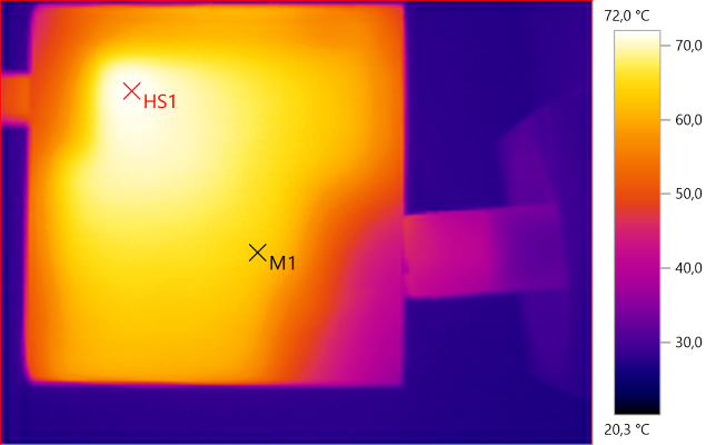
M1: 63.7°C, HS1: 72.0°C
Here HS1 must be the output transistor
M1: 59.7°C, HS1: 67.1°C
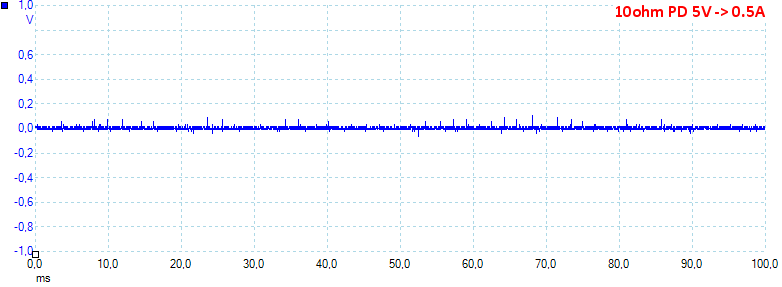
At PD 5V 0.5A the noise is 23mV rms and 300mVpp.
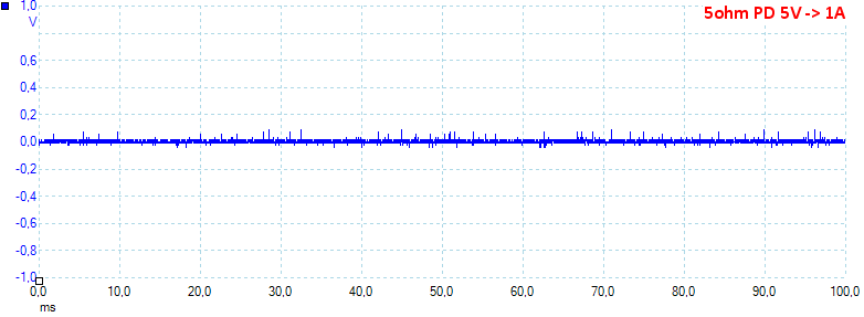
At PD 5V 1A the noise is 12mV rms and 238mVpp.
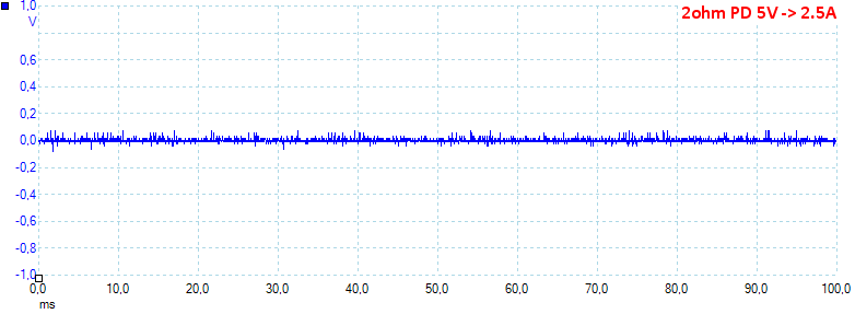
At PD 5V 2.5A the noise is 11mV rms and 233mVpp.
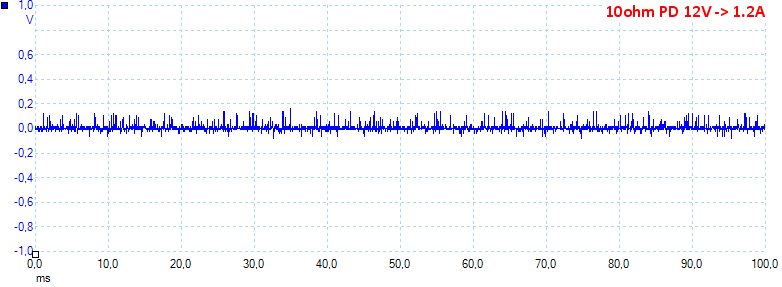
At PD 12V 1.2A the noise is 18mV rms and 304mVpp.
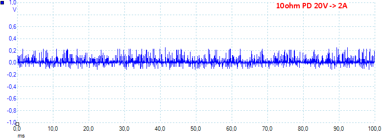
At PD 20V 2A the noise is 33mV rms and 414mVpp, all noise values are fairly low.
Tear down
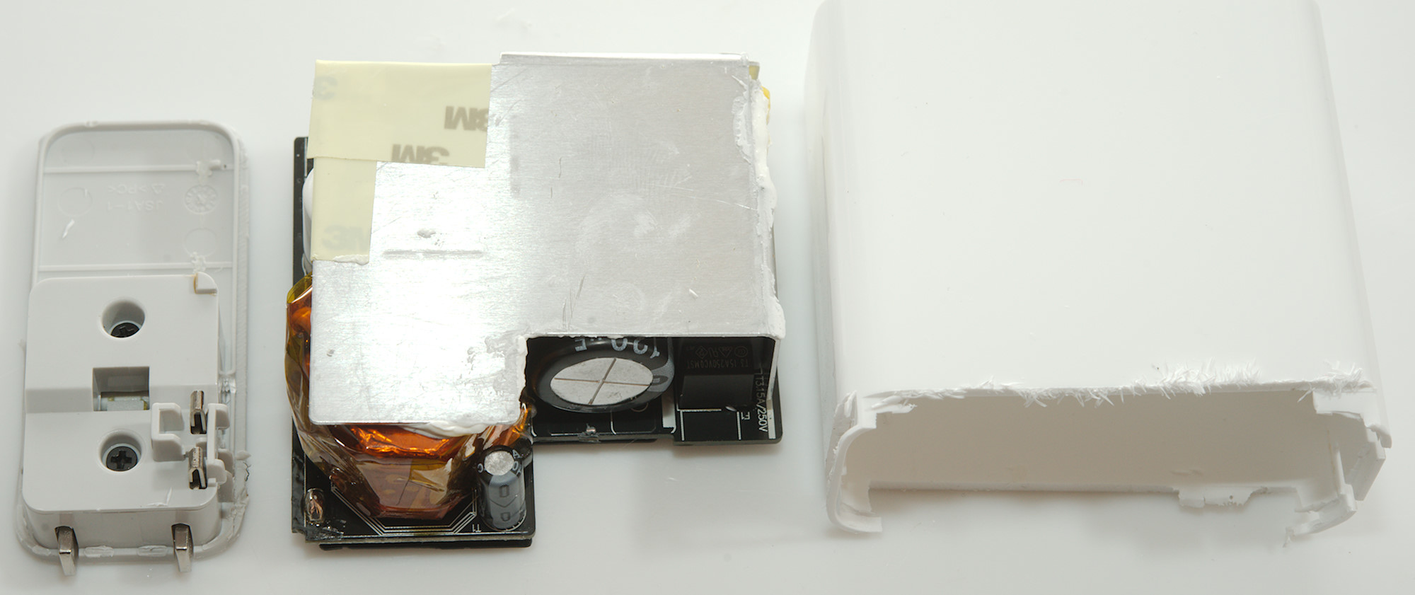
I did not believe I could break it open and went directly to cutting.
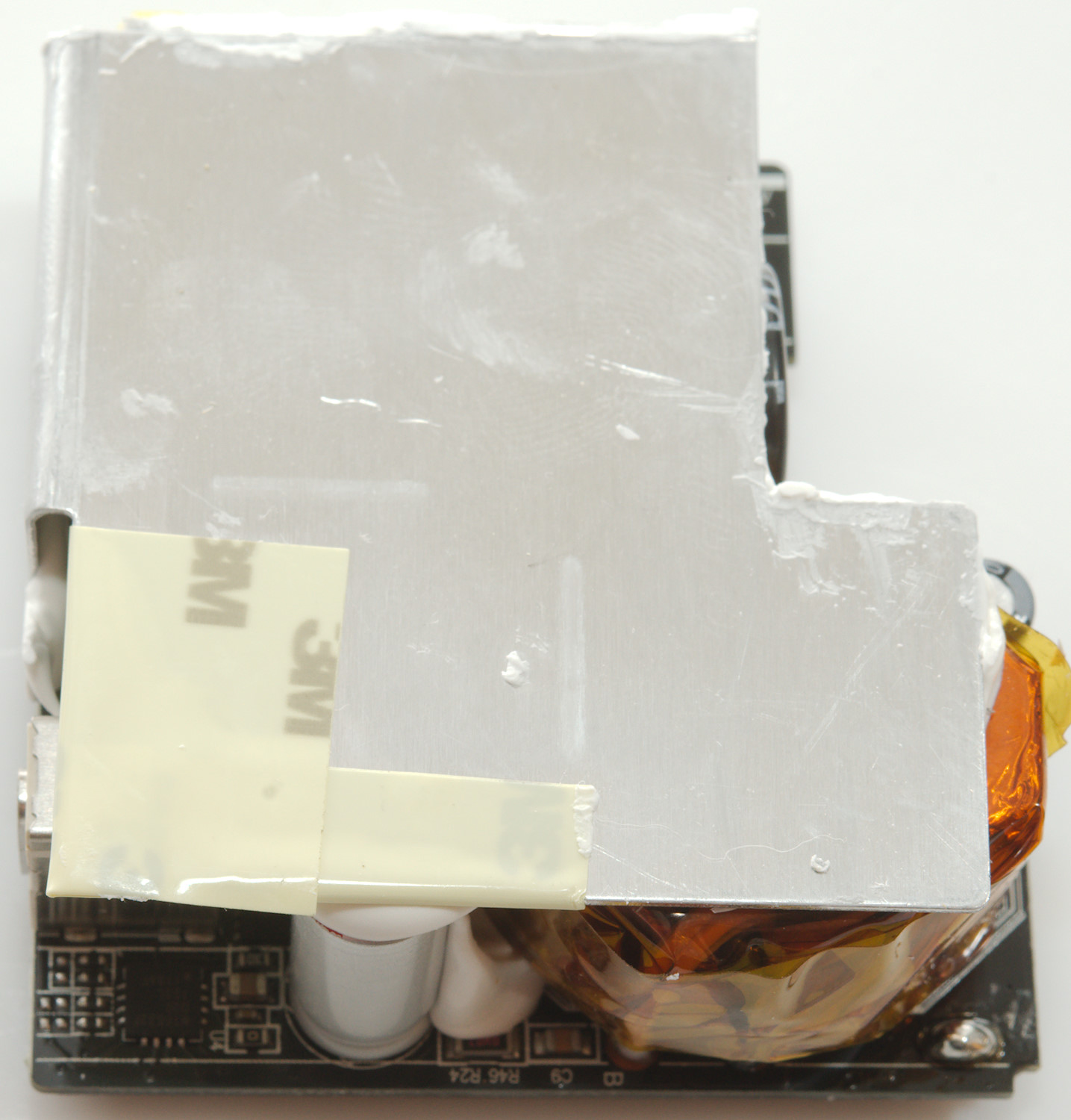
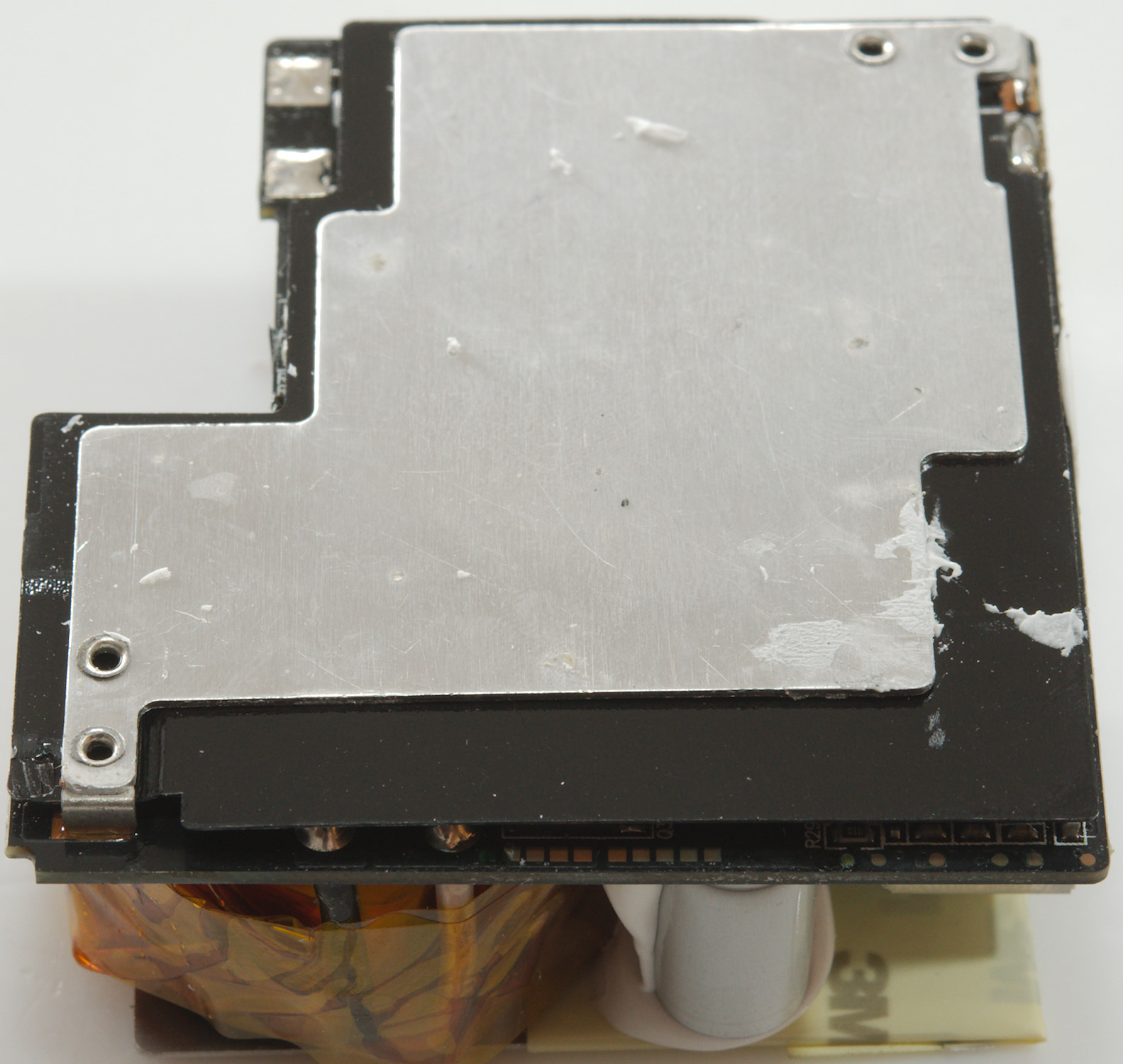
The circuit is hidden in shielding, bit top and bottom.
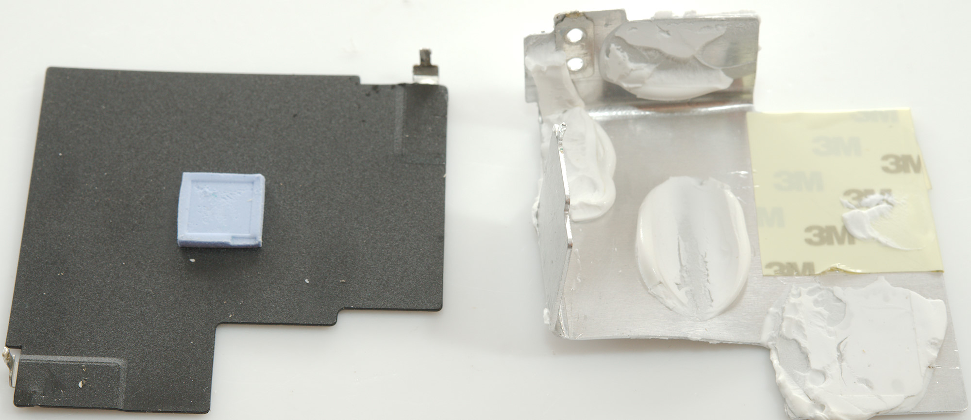
A bit of soldering and breaking and I had removed the shields.
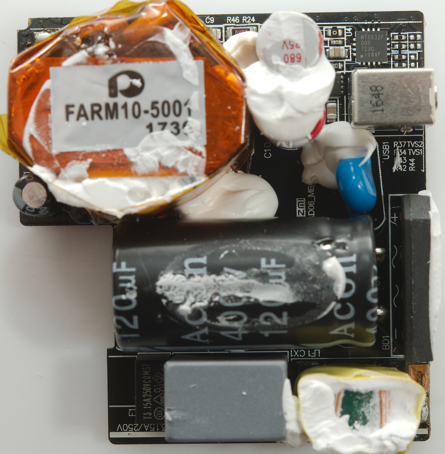
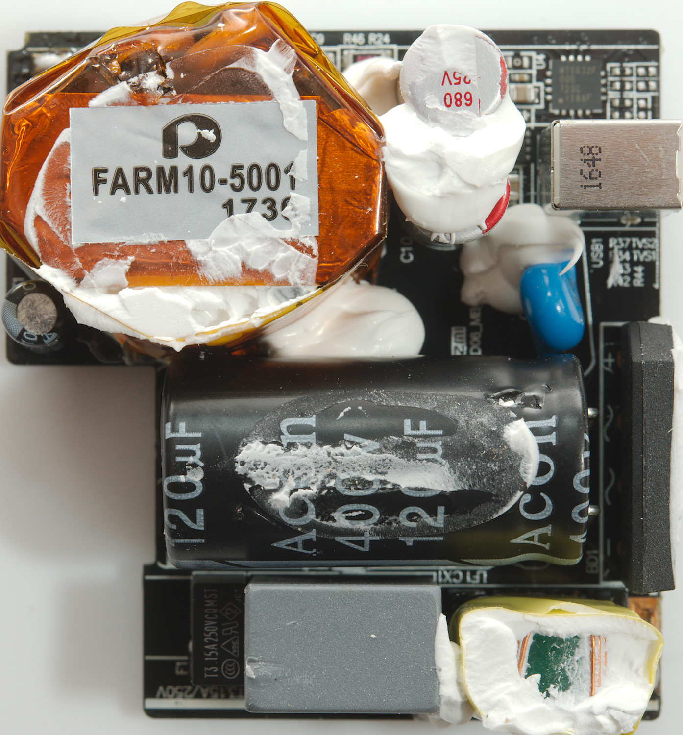
At the mains inpu is a fuse (F1) followed by a common mode coil (LF1) and a bridge rectifier (BD1). Near the bridge is also a blue safety capacitor. On the other side of the USB-C connector is the PD controller (U4: WT6632F S65). The chip behind the usb connector must be a output transistor to enable/disable usb output.


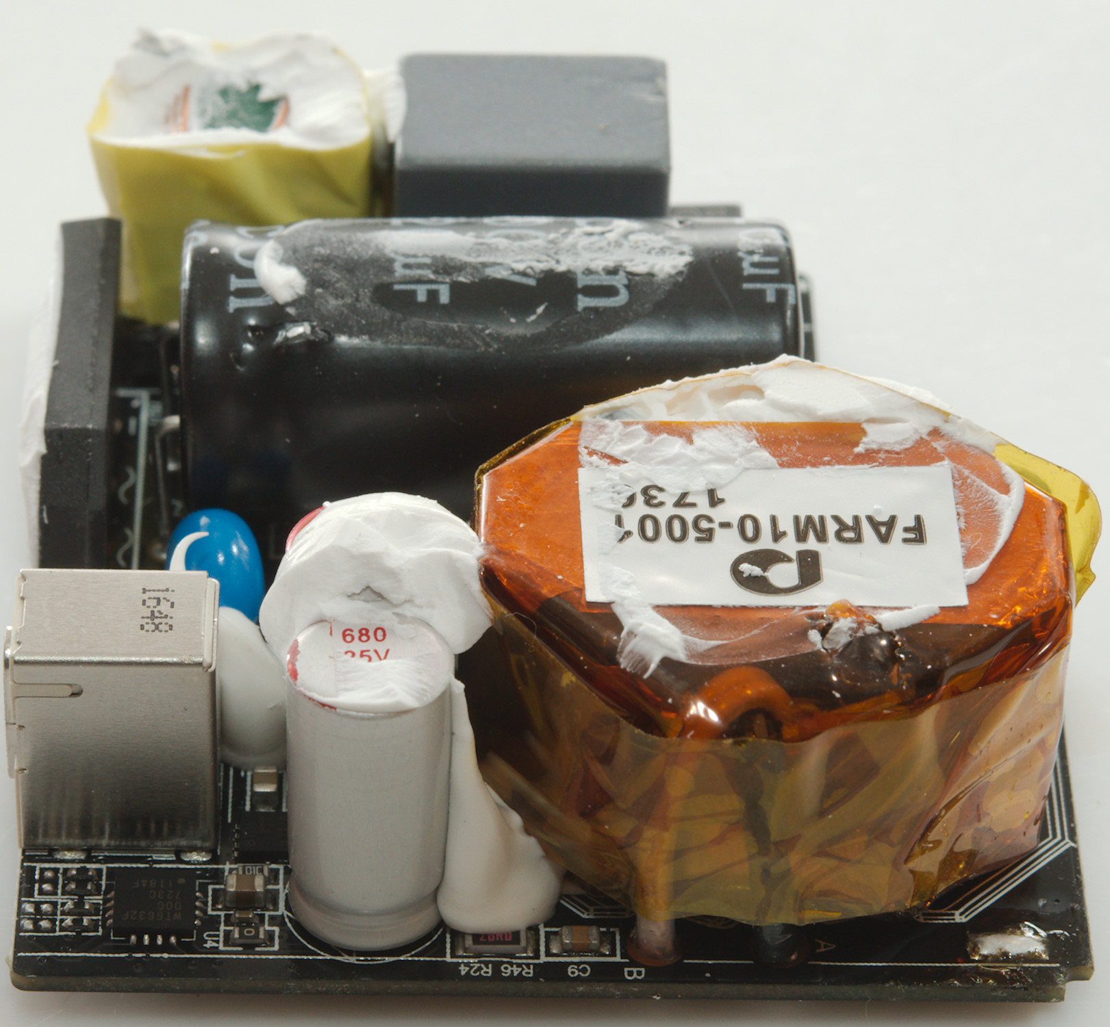
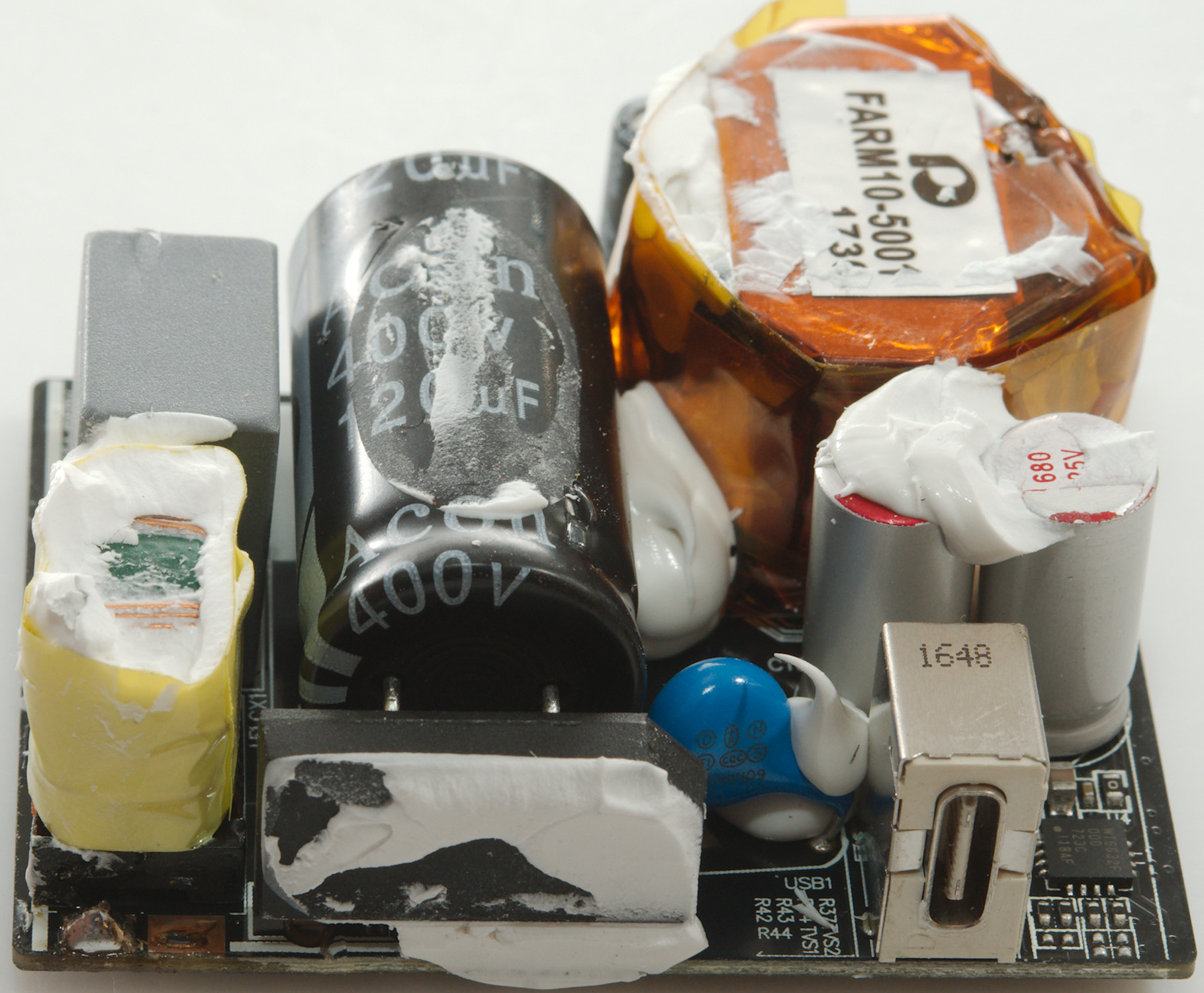

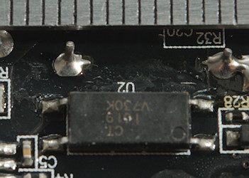
The mains switch transistor (Q1) did have a pad on it for heat transfer to the metal shield, next to the transistor is the switch controller (U1) and the opto feedback (U2).
On the low volt side is a synchronous rectifier controller (U3: Marked ACDDB) and the rectifier transistor (Q3)
I wonder what U5, Q6 and Q7 do.
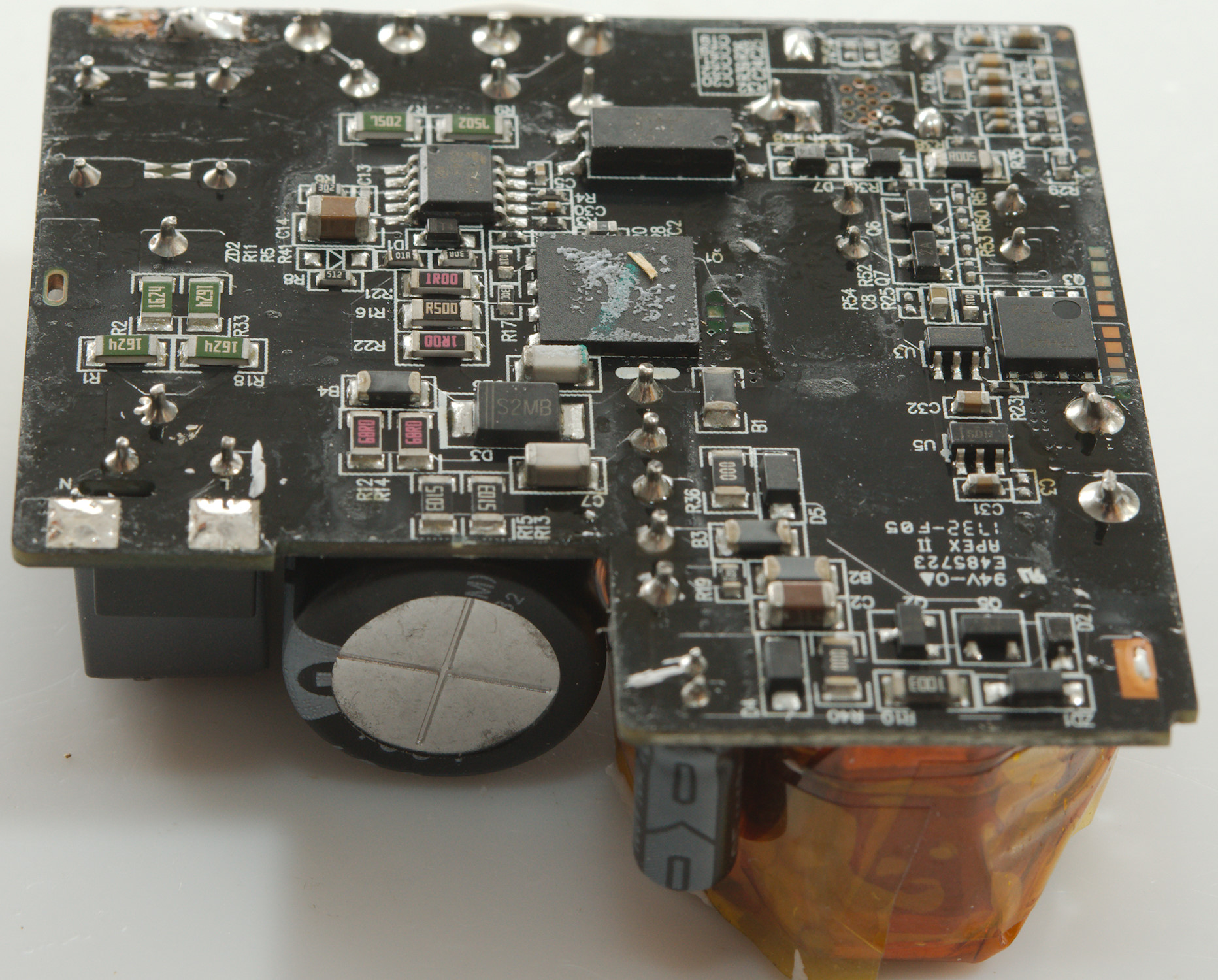
The distance between mains and low volt side is good.
The charger passed the 2830 volt and 4242 volt test, this means it is it is fairly safe.
Conclusion
This is a good PD charger and it can also be used for devices that do not know the PD protocol, but uses QC instead.
With slightly above 3A it can also be used to check if cables allows more than 3A, it is not always marked on the cable.
Notes
Index of all tested USB power supplies/chargers
Read more about how I test USB power supplies/charger
How does a usb charger work?