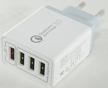
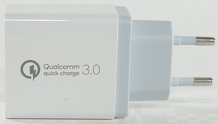
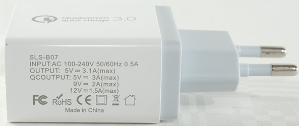
4 port QC3 USB charger SLS-B07
Official specifications:
-
Input: 100-240V 50/60Hz
-
Output: 5V 3.1A
-
Output QC: 5V 3A, 9V 2A, 12V 1.5A
I got it from a reader, I do not know where it was bought.
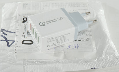
It arrived in a envelope.
Measurements
-
Power consumption when idle is 0.2 Watt
-
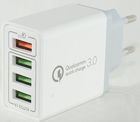
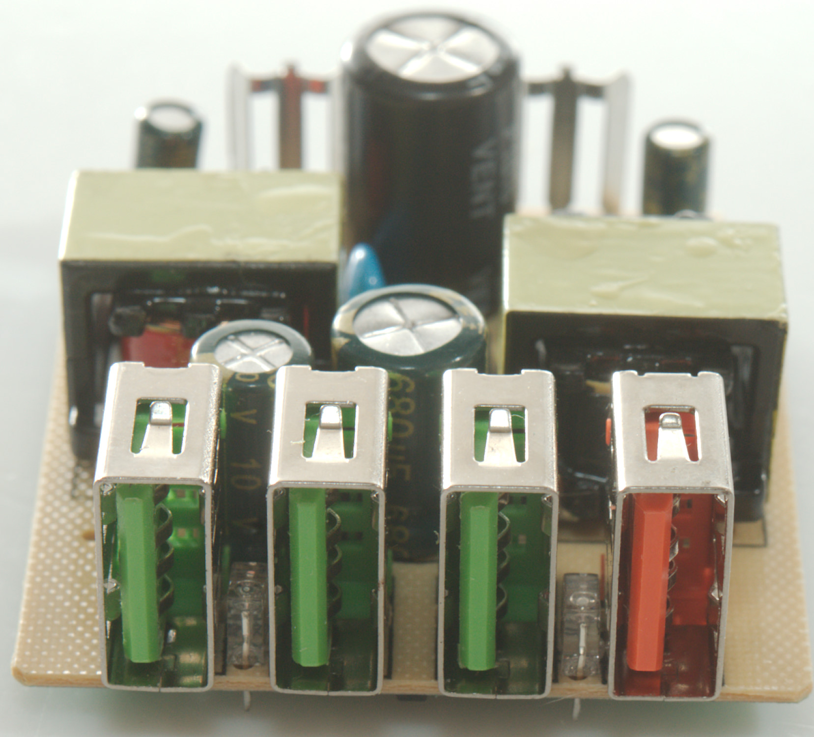
USB coding on the two center sockets auto with Apple 2.4A, Samsung, DCP
-
USB coding on the last is USB charging (DCP).
-
USB coding on QC output is Apple 2.4A, DCP, QC3, Samsung-AFC, Huawei-FCP
-
Minimum QC3 voltage is 3.9V
-
The 3 regular USB outputs are in parallel.
-
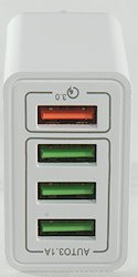
There is some blue leds to light into the USB connectors.
-
Weight 49.9g
-
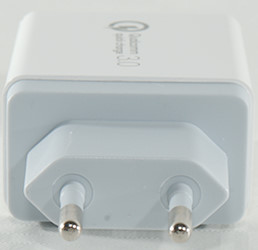
Size: 88 x 45.2 x 21.1mm

A single port can deliver about 2.8A
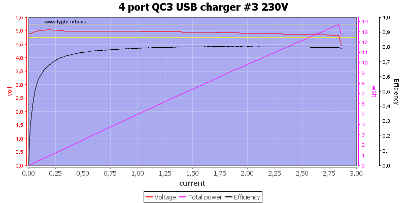
The same on another port.
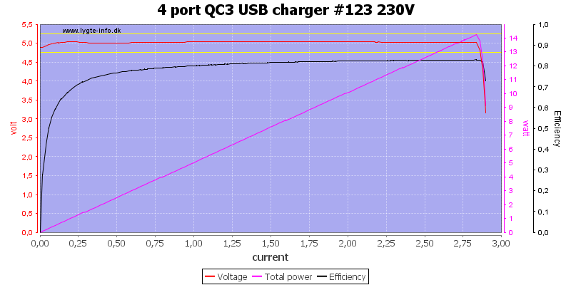
And not very surprisingly the same when all ports are used together.
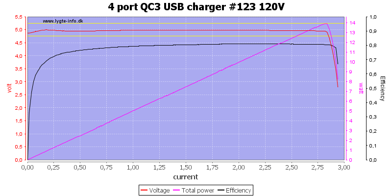
Using 120VAC do not change anything.
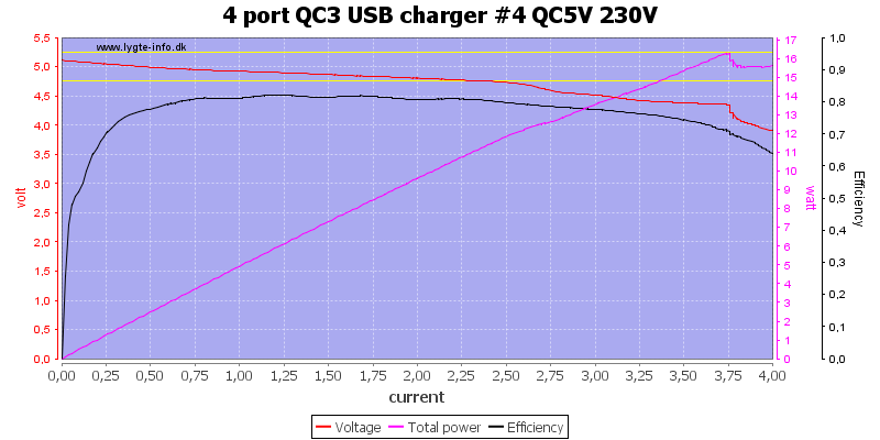
The QC output can deliver about 3.75A before output really start dropping, but it is on the low side at around 2.2A.
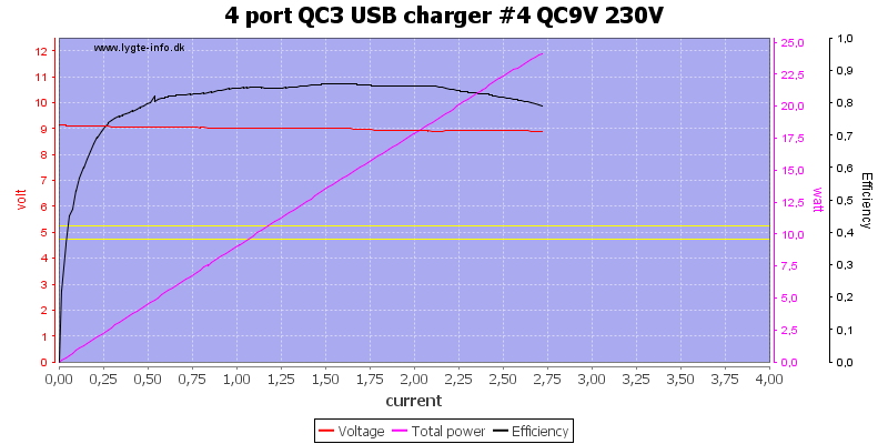
The 9V looks better, here it can deliver about 2.75A
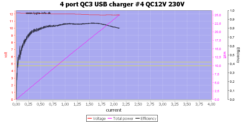
And the 12V QC output can deliver about 2.1A
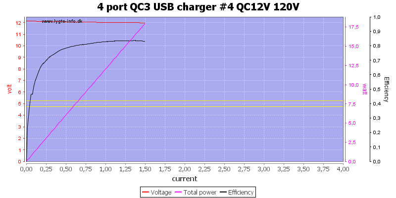
But only 1.5A with 120VAC supply.
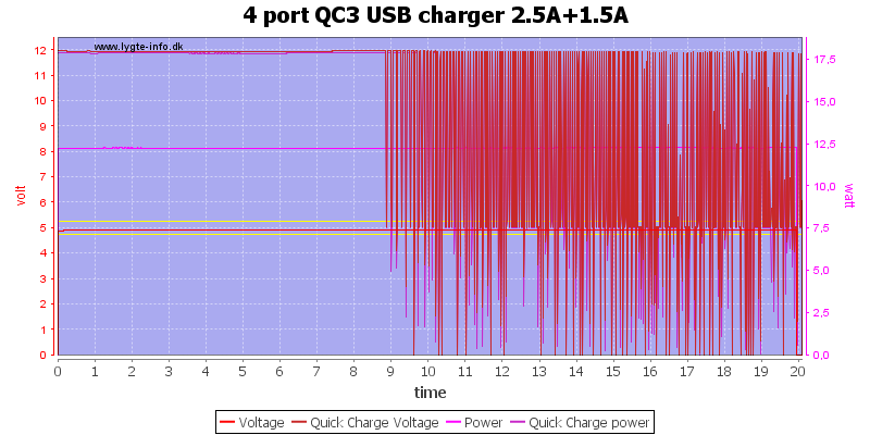
Loading it with rated current, or a bit less on 5V it could only maintain output for 9 minutes.
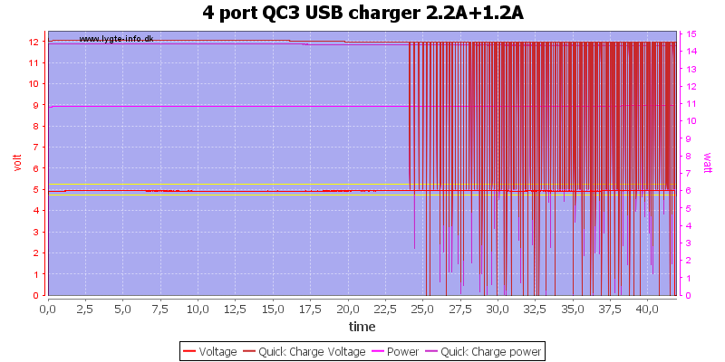
Reducing both a bit did help, here I could run for about 23minutes.
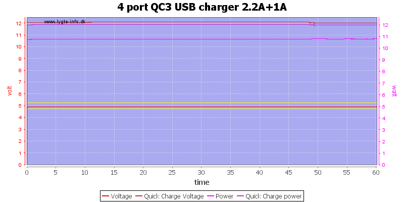
With 2.2A on 5V and 1A on QC 12V I succeeded in running the one hour test.
The temperature photos below are taken between 30 minutes and 60 minutes into the one hour test.
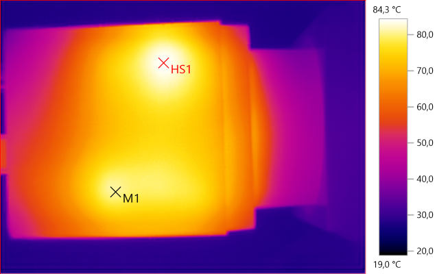
M1: 80.7°C, HS1: 84.3°C
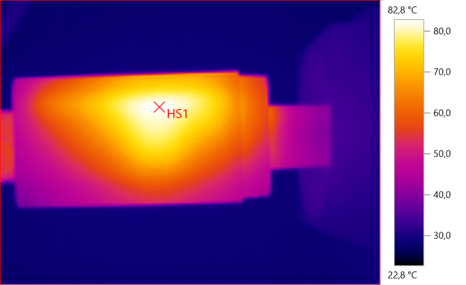
HS1: 82.8°C
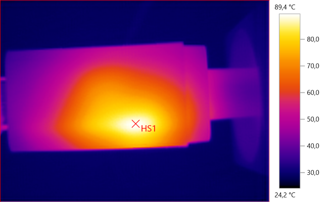
HS1: 89.4°C
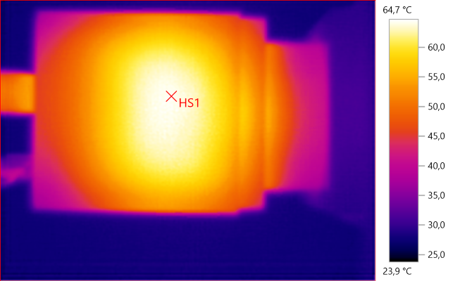
HS1: 64.7°C
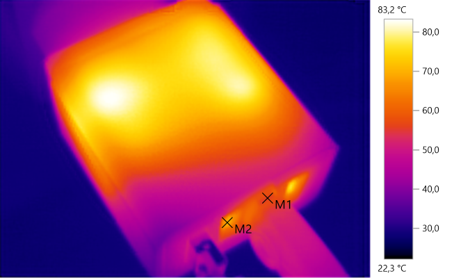
M1: 55.9°C, M2: 69.4°C
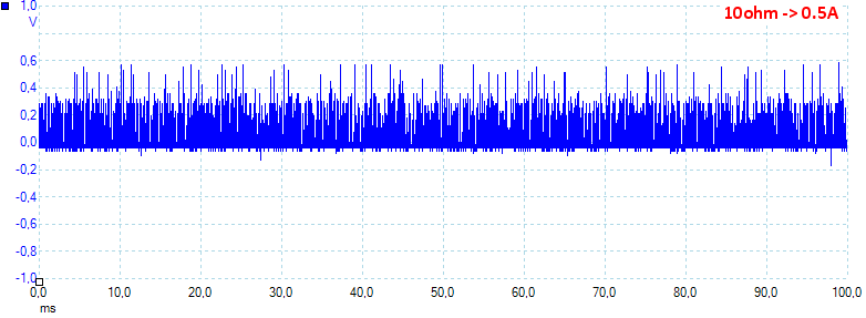
At 0.5A the noise is 105mV rms and 836mVpp.
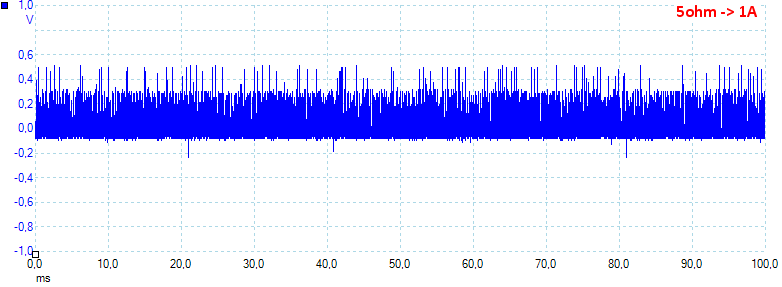
At 1A the noise is 253mV rms and 1541mVpp.
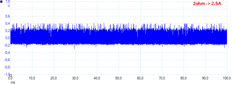
At 2.5A the noise is 159mV rms and 761mVpp.
At 0.5A the noise is 58mV rms and 635mVpp.
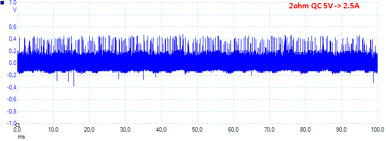
At 2.5A the noise is 125mV rms and 1103mVpp.
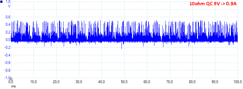
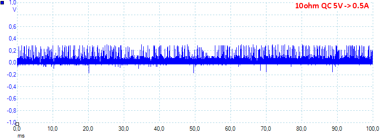
At 9V 0.9A the noise is 104mV rms and 944mVpp.
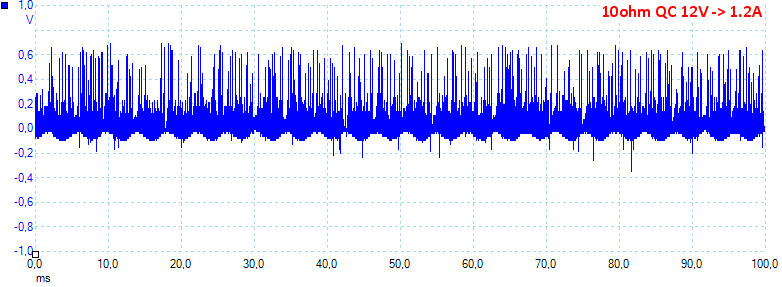
At 12V 1.2A the noise is 137mV rms and 1165mVpp. There is a lot of noise on the outputs.
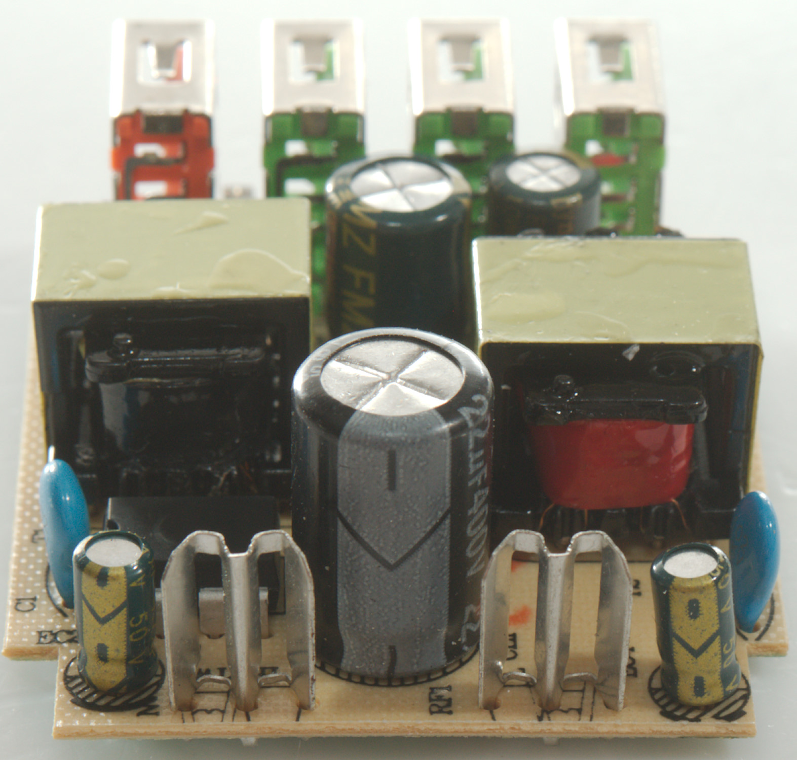
Tear down
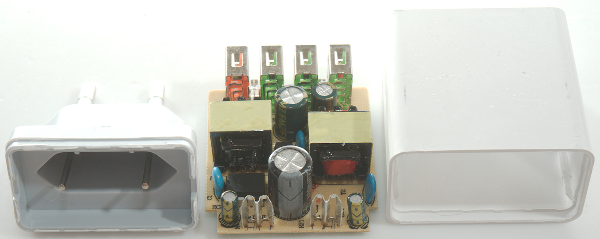
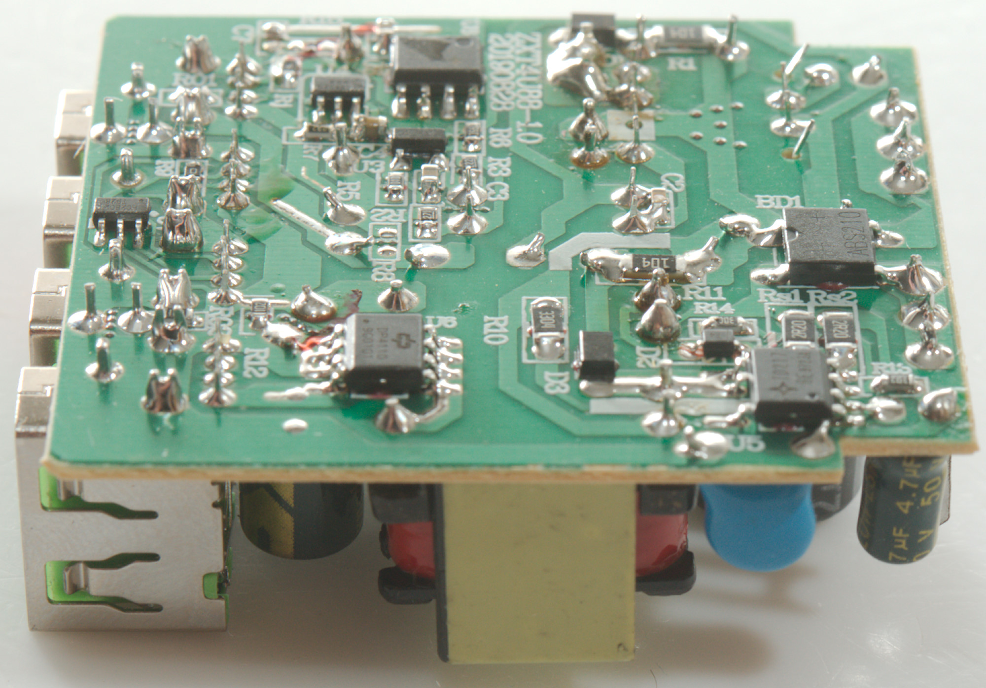
Some pressure with my vice and a knock with my mallet and it was open.
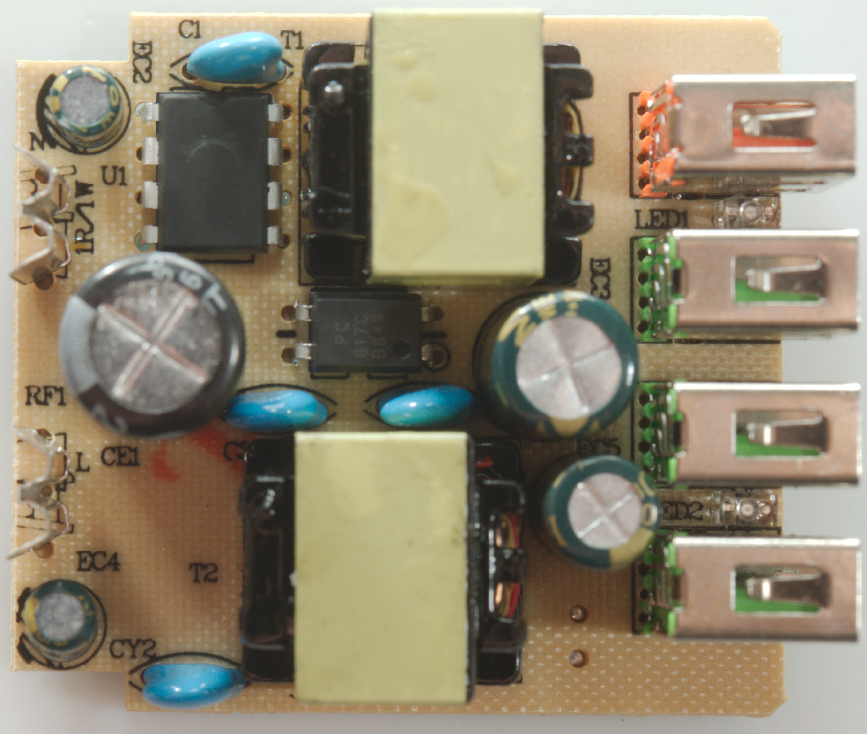
On this side is one switcher chip (U1), one opto feedback, two transformers and two fake safety capacitor (? & CY2: 1nF 1kV).
There is two leds between the USB connectors.
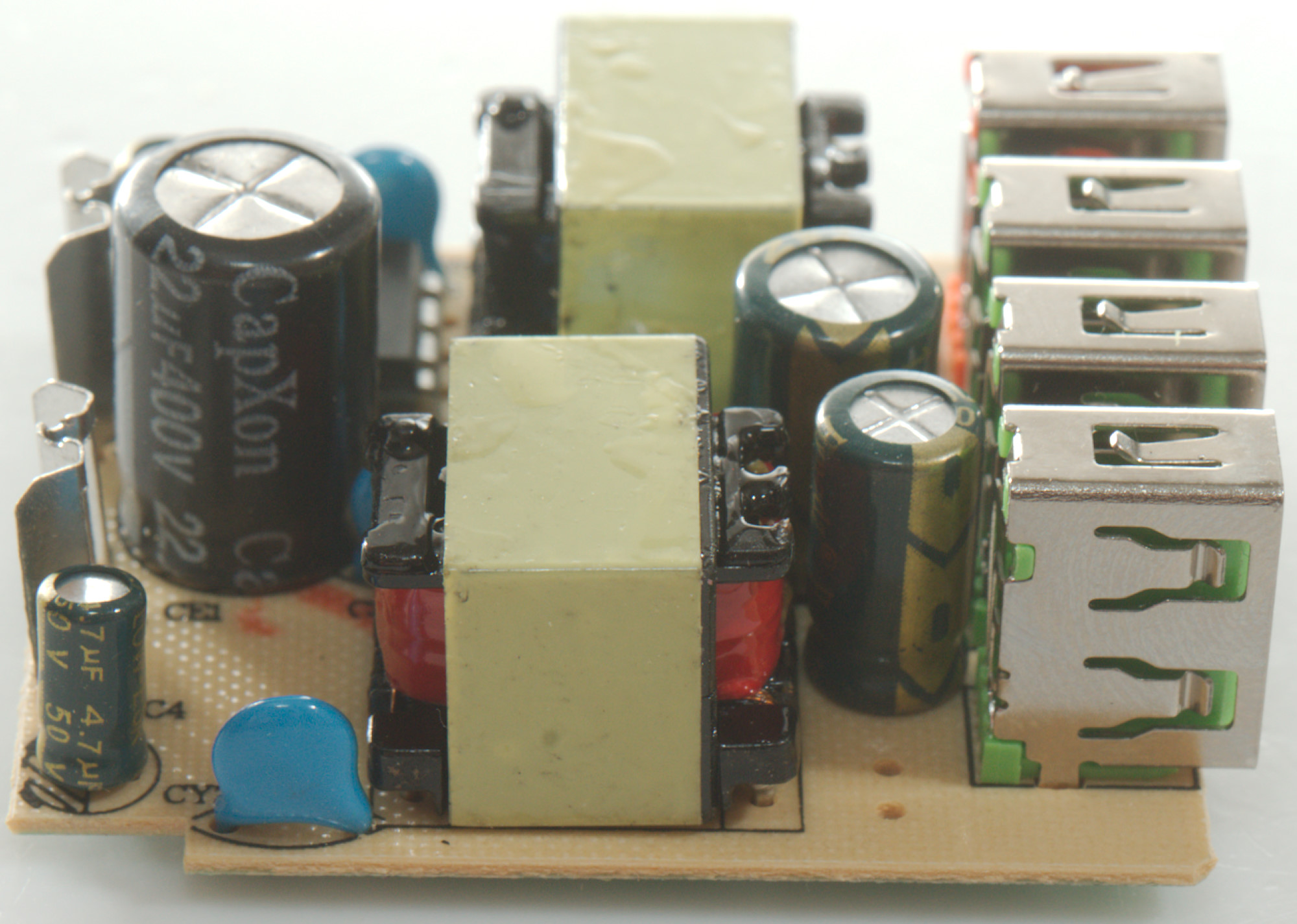
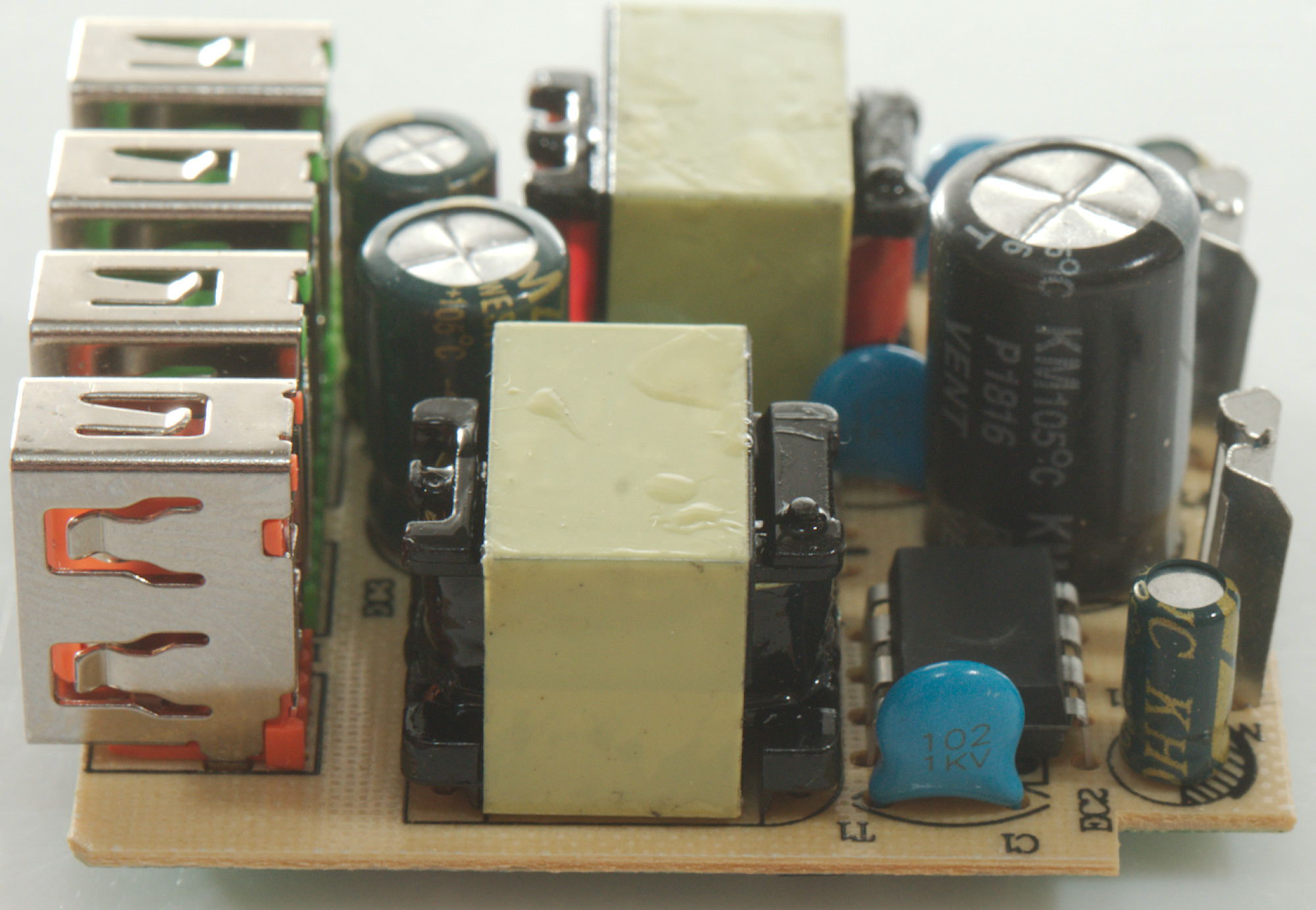
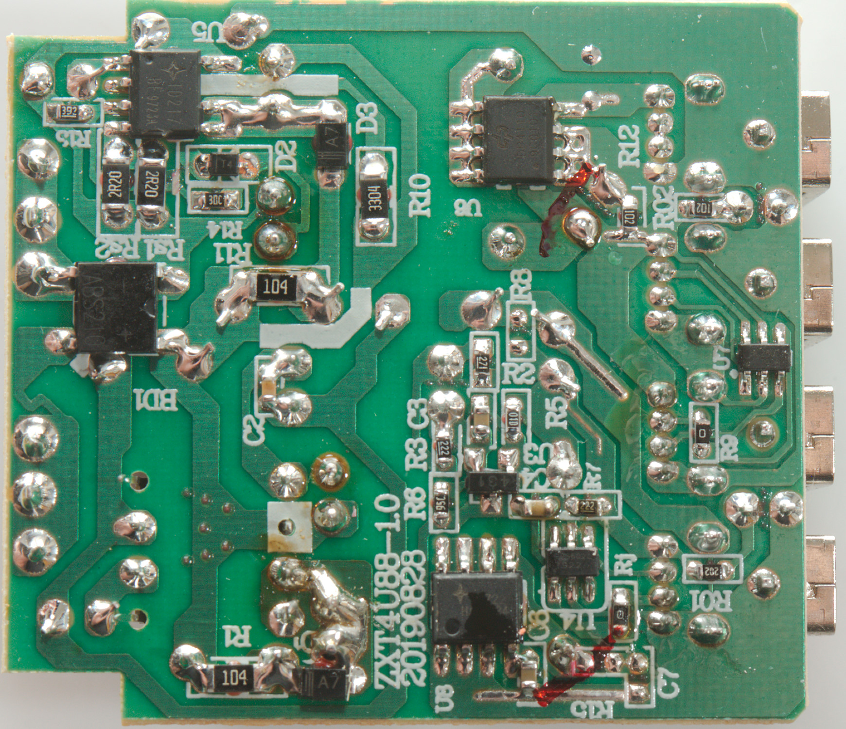
On this side is the bridge rectifier (BD1) and the other switcher (U5: TD217), on the low volt side is a synchronous rectifier for 5V (U6: DP4110) and a dual charge optimiser (U7: HC2802). For QC there is also a synchronous rectifier (U8) and a QC controller (U4: HC6602) and a reference (U3: 431).
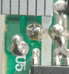
The connection for the fake safety capacitor runs along the edge of the circuit board up into the mains area, this means the creepage distance is less than a mm.
Testing with 2830 volt and 4242 volt between mains and low volt side failed for both. This makes the charger unsafe anywhere in the world.
Conclusion
With fake safety capacitor and very low distance between mains and low volt side there is only one thing to say:
STAY AWAY
Notes
The USB charger was supplied by a reader for review.
Index of all tested USB power supplies/chargers
Read more about how I test USB power supplies/charger
How does a usb charger work?