Hello peoples of the flat Earth. I maked decision, that all my projects must be published (if here is incorrect place for this topic, just let me know where is correct)
Also excuse me for my english. Some times I need to use translator, and the results seems not so correct as must be.
I take 100-150$ for design of the project of PCB for leds (it is really expensive to the MORDOR’s territory, yes, it is joke based on this picture 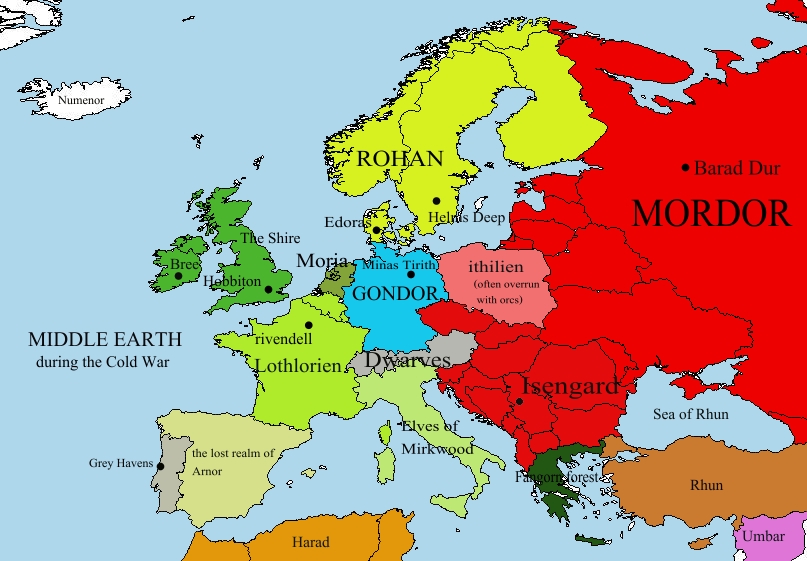 )
)
But I will give all of my projects for free here (also projects what was designed for money, I already asked customers about publishing their projects for free)
In this time all files (with 20+5 projects) will be in one .7z archive (.lay6 final and previous versions of pcbs and stencils (SS), .png preview pictures, some .gbr files ready to go to producing)
You can download it (40mb) here yandex disc
or here mail.ru cloud
or here goodrive
password is: password
Inside is:
2-5050
3-353025
4-5050
6-2835ccr
6-3030
6-3030ccr
6-353025
12-3030
12-3030-64
12-3030ccr
14-3030
36-3030
36-353025
42-3030
48-5050
60-2835
108-353025 v2.2E
BA15S
C5W
W5W
SS Stencils
t8-3530 (future project)
t18-2835 (future project)
t18-3030 (future project)
t36-2835 (future project)
t90-2835 (future project)
PCBuv (not my project for nail lamp with 3 types of uv)
I will add info later, but:
5050 LEDs (I use it for grow blue, red, white leds):
The main idea was to using more chips in the same square, also I find that they already can be with 60-80° lens (was 120°)


48-5050 73.2021 Ø73mm


4-5050 79.2021 Ø23.4mm (I just finished it and I have time to start this topic and prepare files to publishing)


2-5050 october 2019 22x22mm (need additional space to V-cut)


3030 and 2835 LEDs (it is possible to solder 3030 leds in 2835 contacts, and 2835 in 3030 pads)
6-3030ccr 330.2020 Ø23.4mm


6-2835ccr december 2019 22x22mm (need additional space to V-cut)


6-3030 november 2019 22x22mm (need additional space to V-cut)


12-3030 74.2021 64x12.5mm


12-3030 november 2019 99x12mm (need additional space to holes)

12-3030ccr november 2019 99x12mm


14-3030 december 2019 100x86.6mm (idea was to change CCT and do not use additional heatsink)


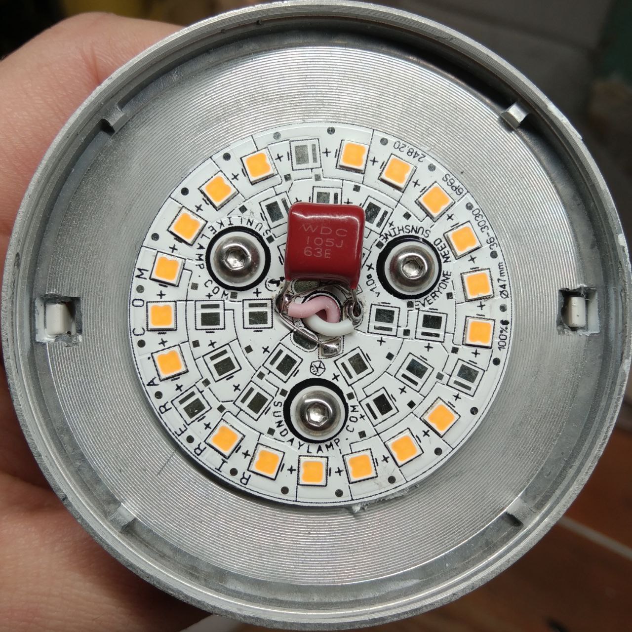
36-3030 248.2020 Ø47mm


42-3030 288.2020 Ø110mm


60-2835 245.2020 Ø65mm (at first it was project for 75 leds)


For vehicles with 3030 leds:
BA15S


W5W (T10 T5)


C5W (T11)


3535 3030 2525 LEDs:
108-353025 may 2019 73x63mm copper base (idea was to combine 3535 3030 2525 leds with switching modes)


6-353025 october 2019 (can be 2S3P or 6P, also need additional space to V-cut, next will be for 8pcs project)


p.s.
FastFAQ
0. How to draw it?
- I use Sprint Layout 6 (I think that after 4 year of using it I draw it like a god, but it takes 5-20hours for 1 pcb and every project need some little changes after some days or hours of analyzing what the final is) after the drawing need to export holes (3.3 format of .drl) and layers (mask, copper, silkscreen, outline) to gerber format (.gbr)
- The most important was to understand the limitations of PCB manufacturing technology. For example, that the V-cut has a certain width and the manufacturer (hi to allpsb :rage: ) does not add the distance between the boards even if the blade goes on the track, and we will know this only after receiving the board (1.5-2 months in my case). Also the distance between the tracks. This is all done experimentally. Now I use 0.25 0.3 0.35 and rarely 0.4 mm, although there is a chance that they will still increase the distance to 0.3 mm, although at 0.25 mm they did not warn me about increasing the distance. You also need to know the error of the holes. Contact pads also have a margin of error. Also in silkscreen printing. I think that different manufacturers have a different margin of error, but approximately the same.
- 0.25-0.3mm between near roads, and 0.3-0.35mm between further (36-90v). Error rate of the hole maker is ~0.35mm, so it need to be 0.5-0.8mm space. Outline I recomended 0.5-0.8mm. The outline cutter is quite accurate, but it leaves a ~0.2 mm notch where it enters or exits. But even if the milling cutter or V-cut touches the track, this does not mean that there will be a short circuit to the base of the board in that place. But this can be dangerous if you do not use transformer type of led drivers, but throttle power supplies. I prefer to use transformer ones, they are safer.
- marks: version, date in format № of the day and year (yes, someday people will develop to a 5-day working week), size of the board, quantity and types of leds, scheme (for example 4P3S), nominal costs of the money (Grower) based on ready pcbs (copper, or cheapest aluminium 1.6mm 1oz and etc)
1. Where ordering PCBs and Stencil?
- I used allpcb, but I do not like it anymore =( I back to my previous manufacturer in China. You can contact with him by email hq.niu[D0G]pcbsmart.com
- Stencil in the same place, but in the jlcpcb some chipper (under 4000 holes to 290x190mm space 380x280mm size with framework)
2. What parameters?
- Stencil 0.08mm thick much better than 0.1mm, costs additional ~1.5$
- PCBs parameters what I recommended:
- 2oz (ordinary copper layer is 1oz = 1.37mils = 0.0348mm)
- 2mm of the aluminium base (ordinary 1.6mm)
- Heat Conductivity parameter 2w (ordinary 1w, but I think that they use every time 2w boards)
- Surface Finish: HASL Lead Free! (without lead! Because it will crashed with 138° soldering paste)
-Mask: ultra white (high reflectivity) mask (it is much white than ordinary, ordinary white seems like gray if compare it) - no V-cut or add additional 0.3mm in the each sides (blade is ~0.6mm)
3. How to solder leds.
- I use thermal table 946C+ It is cheap, but shipping can cost much

- First time I was soldering on an iron. Just use copper or aluminium buffer plate. And set minimal possible temperature (145-150° if Sn42Bi58) for your solder.
- I use 138° lead free solder paste Sn42Bi58

It already has the right flux. It should be stored in the refrigerator. And preferably in 2 or 5 ml glass syringes. With such syringes, it is convenient to use it

The oxidized paste leaves a lot of dark lumps that do not melt. This paste is better not to use.
- It is necessary to solder without sudden cooling and heating to prevent cracking of the solder of the LED and solder of the his crystal.