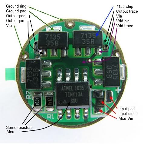
Recently I have been attempting to modify a7135 board to allow it to run on series connected li-ion batteries instead of single or parallel batteries and during my searches and posts many terms come up that some readers may not know. What exactly is a “trace”, or “via”? Which pin is which? I thought it would be helpfull to show a sample board(copied from a Hikelite post) identifying various parts to use as a reference when discussing mods. I plan to use it or similar pics myself. I am just learning to use paint.net so please excuse any inadequacies in my efforts.
Here are some definitions: Solder mask- The green paint that covers the board and the traces. Trace- The copper strips that connects different pads on the board. Pad- The solder spots that chips, wires, and other components are soldered to. Chip- The multi-legged bugs that do the work on a board( in this case mainly 7135’s and Attiny 13). Pin- The metal tabs that are the input, output, ground, etc. connections on the chips. Input pad- Where to hook up the battery + and led + wires(also connected to center pad on other side). Output pad- Where to hook up the led - wire. Ground ring- This connects to the battery - wire and any slave boards. Vdd- This is the control that allows the Mcu to turn the 7135 chips on and off. It’s how the modes created in the Mcu are translated into current in the LEDs(also connected to any slave boards). Slave board- A board “slaved” to the mcu so that additional current can be fed to the same or additional LEDs. Via- The tiny metal plated holes that form connections to the traces on either side of the board. Input diode- This provides reverse polarity protection for the mcu. Jumper- A wire that links two pads or pins on a board.
Each board will have a layout unique to that series. A 105C will have different traces and some different resistors and capacitors in different locations from an AK-47 but the 7135 chips are all the same in the layout of the pins so once you understand how the traces connect the various chips the similarities of the boards become obvious.
It might be nice to have a place to find various boards that identifies the parts that make up linear, boost, and buck drivers. The first really excellent photo of this type that I saw was in the Oldlumens/Techjunkie thread on paralleling slave boards.
Here are some links(in progress) to info on the following:
AMC 7135 data sheet, get the real dope here. Removing chips, see how its done here. Stacking(piggyback) chips, see post #10 in this thread for tips here. Stacking boards, here, and here mod. Oldlumens/Techjunkie master/slave mod, really good thread, here. Series led mod, link to CPF Download’s Poorman’s Multilux thread here, if you dare! Series led mod, link to BLF Rufusbduck thread here. Bring plenty of coffee, I am not succinct. Heat sinking chips, from the Rufus thread here. If there are others posted I can add them as well. Heat sinking boardshere, see post #23
I'm not electroncally minded but this helps a lot. I have ruined my share of these boards somehow and even tried piggy backing the chips. For someone like me and I guess many others this is a great help in simplifying things.
I hate to derail a thread this early in the game, but I’ve been confused about one thing recently and think maybe it’s an easy/obvious answer that I somehow missed in my googling.
So, to show my ignorance, here it is: with different leds wanting different forward voltages at different current values, how does a constant current driver like this “know” what to feed the led?
(If this is really basic electronics and you can provide a link to a good primer, that would be appreciated.)
When piggy backing 7135 chips, are all three pins on the new chip connected to the corresponding pin on the bottom chip? Does it matter which 7135 chip you piggy back onto?
Truth is, the board doesn’t “know”. You pick the board based on the drive current you want. You can also add or remove chips from an existing board. Each 7135 chip adds 350-380mA to the boards total output. 4 chips on one board gives 1.4-1.5A, 8 chips on one board gives 2.8-3.0A. As long as the battery voltage is above the forward voltage of the emitter, each chip will pass that 350-380mA and turn any excess voltage into heat.
Edit- This forum is the best primer but just to add, forward voltage is a range for each led and fluctuates with heat. The same led will have a higher Vf at 1A than at .5A. Just keep asking. People here happy to answer
The middle pin is the same as the ground tab so if you solder the tab you don’t need to solder the middle pin.
Matching the pins is what you want to do to add more chips in parallel. They do not connect in series.
It does not matter which chip you stack onto other than ease of soldering when you are adding more than one chip and are right or left handed(or ham handed like me).
here's my clueless question: I see in the picture that the Ground Pad touches the Ground Ring, which is continuous with the flashlight body? In other words, the Battery (-) = PCB Input (-) = Ground Ring =/ PCB Output (-) = LED (-) ? If it is true, I can't wrap my head around the fact that the whole Negative terminal is continuous from the battery all the way to the LED. edit: got it, the 7135 sits in-series between the ground and {PCB output(-)=LED(-)}
Led- is NOT the same as the ground ring. The led- pad connects to the left hand pin of each chip. When the mcu applies voltage to the Vdd pin on each chip( from the Vdd trace) the chips “turn on” allowing 350 mA to flow through the chip from led- to ground. 7135’s are often described as smart resistors but I prefer to think of them as constant current TRANSISTORS when describing how they function.
The chips are all parallel wired. The LED, battery and atmel EPROM cant tell which chip is double-stacked and which is not. So it makes no difference.
Having just completed a 10X double stack mod on these, I had a VERY hard (impossibly hard) time bridging the solder pins between the stacked chips. I just could not get the soler to “jump” down. Yet I was able to very easily accidentally bridge solder over sideways onto adjacent pins. Very frustrating to say the least.
Then I remembered someone (andi or E1320) suggesting to bend the tabs down. That did it!! The tabs are long enough and reach far enough to make perfect contact with the bottom chip. They are soft enough to bend easily with no ill-effects to the driver. Once I nailed that, I finished the mod in ~15 minutes…. and FWIW I am only using a moderately-fine tipped pencil iron. I will definitely be doing more of these mods in the future. FWIW my drivers are the ones with the stars to configure the mode groups.
I also found it MUCH easier double stacking the chips on the battery side of the board. Its just the 7135 drivers and the +B spring. No other SMT stuff to get in the way of my shaking hands.
Rufus THANKS for doing this!! There are so many threads on these drivers (and their various flavors), its hard to keep track of them all.
The middle pin and the ground tab are the same bit of metal. As long as the outside pins are matched up correctly, whether you solder the middle pin or the ground tab is not electrically important. A slightly better heat connection would be soldering the larger ground tab and clipping the middle pin makes a bit more room but the main thing is like to like.
Not burned off as heat. Do you know how a FET works? You can have a different voltage on 1 side than you do on the other, it is not burned off as heat though.
Don’t know about Field effect transistors. I thought 7135’s are constant current sinks that turn excess voltage into heat. The reference to transistors was comparing the Vdd pin to the “gate” of a transistor. Just looking at similarity to what it does as opposed to what it is. For perspective only.
The bolded statement is correct. 7135 chips DEFINITELY run hot pushing low Vf emitters with 4.2Vin. They generate enough heat to be “painfully” hot to the touch after ~.5-1 second of gentile touch pressure…. IMHO hot enough to require additional cooling methods.
Agreed. The data sheets seem to indicate the possibility of handling up to 4V excess(see dropout voltage vs output current graph) which translates to ~ 1.5W PER CHIP. Also indicated is the heat sink area at various thermal resistances. Up to 1000mm^2 of copper trace area to sink each chip. WAY more than is present on a 17mm board. I have often wondered how much better the chips would do if they were not backed up against another high heat source like the LEDs. I have always tried to separate the led and the driver as much as possible even though it adds some extra wire.
I recently did that on a build. The 7135 drivers were so hot I could not keep my finger placed against them for more than a second without pulling away from the pain. The 10x7315 chips got very hot MUCH quicker than the XML running at 3.8A. I added cooling fans and pieces of 22AWG solid opper wire to try and sink and radiate heat away form the double stacked chips.
I have always wanted to try making my own driver “board” by using 10x chips, 20-22AWG solid copper wire and stringing the drivers in a row parallel wired.
Better question - Do You know how a FET works? You can’t simply have a different voltage on two sides of anything without it acting like a resistor (Ohms law Applies) and a FET is really just a variable resistor when being used as a current limiting device (AMC7135). If you draw 350mA through a FET and one side of said FET is at 4V while the other is at 3V, then I promise, 1V * 350mA = 350mW is being dropped and converted directly to heat. In that situation, the FET is being gated to act as a 2.85 Ohm Resistor.
Even the datasheets of a FET will explain this. At different gate drive voltages the RDS (Resistance from Drain to Source) changes. This is how the AMC7135 functions - the control logic varies the FET gate voltage in order to maintain a RDS value that allows 350mA (or 380mA) of current to flow.
I do know how a FET works, but it’s been a few years since I’ve looked at them much, but you are right. I think I was actually thinkin more of a BJT anyway and in an amplifier situation i.e. an audio amplifier where you aren’t controlling to a constant current etc.