10mm linear driver- discussion thread now

Below is a list of members who have expressed interest in a thinner(.8mm) board or just responded in the thread with soft numbers next to them. At the moment, there’s enough I interest for me to justify ordering 100 boards but only those with a number next to their name are assured of getting them. Anyone else would be first come first served until they are gone.

The conus price is $.70 each plus $1 for postage, packaging, and paypal for up to 10 pcs then $.75 each plus $.75 for p, p, n p. For orders over 10. Aussies get yours from Mattaus and contact him for pricing etc. I’ll send them anywhere they’ll ship to but you pay the postage. I have about a hundred of them with about half spoken for. This works out to $8 for 10 of them.

USPS 1st class for 1 oz is $1.15 so outside Conus it’s $.70 each (up to 10 pcs) plus postage, packaging, and paypal fees of $1.65. This works out to $8.65 for 10 of them.

Aussies:

Mattaus - 20, 50 shipped to Matt, received
MRsDNF - 6, see Matt
Ejected Filament - 6, see Matt

USA, EU

Me - 100 less …
Djozz - 5, pd, shipped, received
WarHawk-AVG - 10, pd, shipped, received
DBCstm - 10, pd, shipped, received
Texaspyro - 6 10, pd, 4 more shipped, received
Helios
Sirius
Ima4Wheeler - 10, pd, shipped, received
richnpc - 10,pd, shipped, received
Nickelflipper
ruffles- 5, pd, shipped, received
Nitro
Peetz - 10,pd, shipped, received
Jalben - 10, pd, shipped, received
Koyotee - 8, pd, shipped, received
Lithium - 5, pd, shipped, received
Firelight2 - 5, pd, shipped, received

12 mm boards

V 2.3 this is the current production model available from Oshpark 10.5mm and coming very soon in a .8 mm thin board.

V2.2

V2.1

V2.0

V1.0 Have a look!

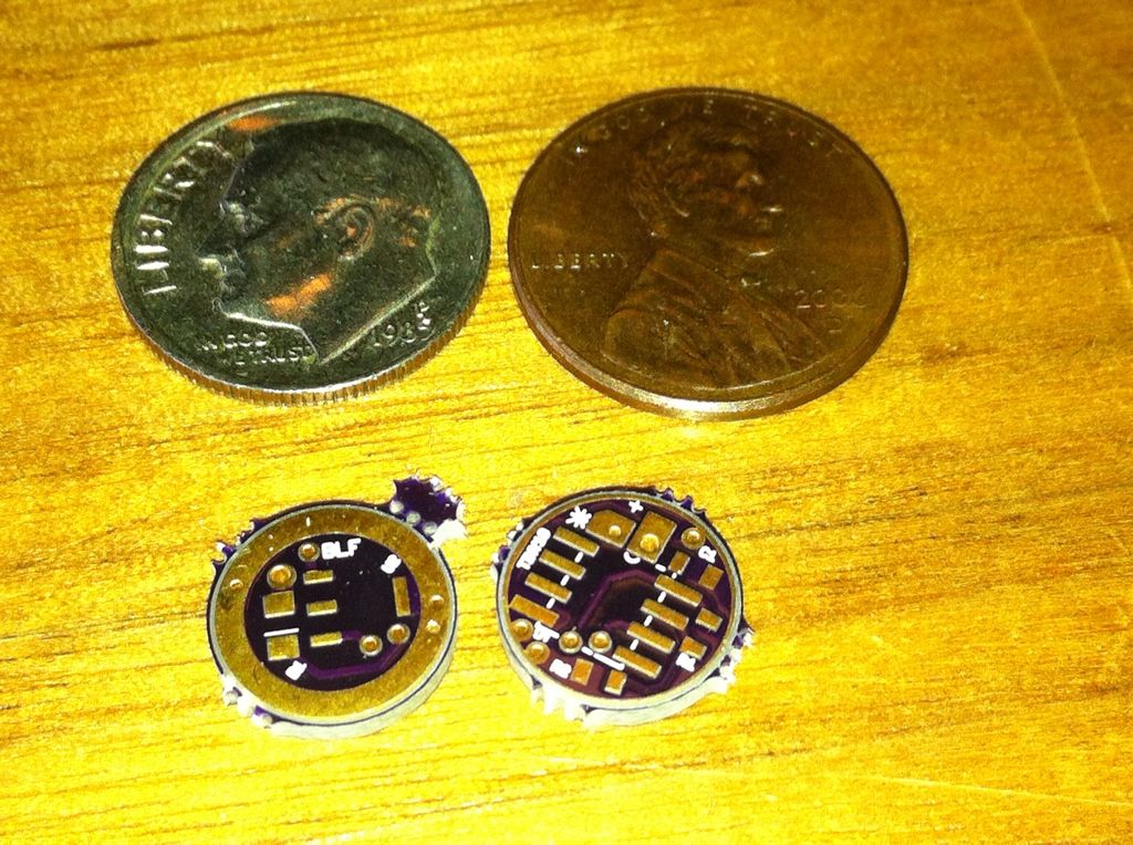
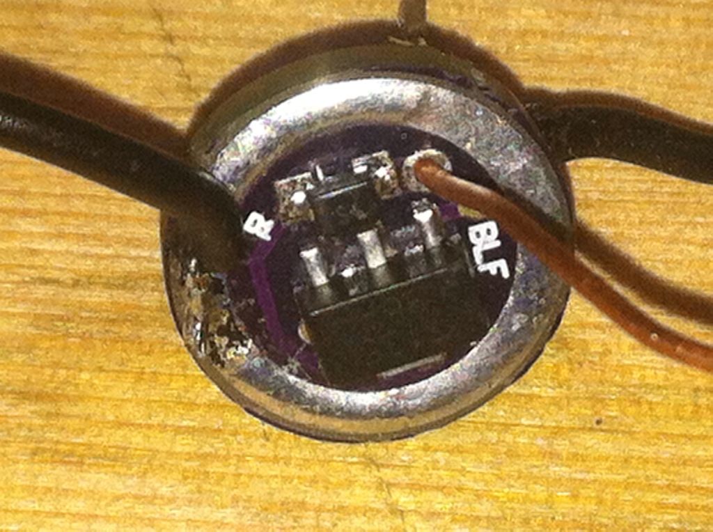
As per request, here are a few pics of the driver w/transplant components. As you can see, my smd soldering isn’t great but it is good enough to work.

As soon as I get a chance(after MRTdiver’s Minimag is done) I’ll attempt to load one of these. DBCstm gets a try as well but there are only 6 boards in this first run so only insane dedicated diyers need apply for a chance at the remaining beta boards.

Just to be clear, one(or a stack) of 7135 chips gets soldered to the ground ring side of the board along with D1. On top of that a B+ contact plate needs to be located with a contact wire running through the board to led+. All of the other components of a nanjg 105C board(mcu, C1, R1&R2, and led-) fit on the other side of the board.

The purpose of this is to have a dedicated liion driver( not some “maybe it’ll fry, maybe it won’t” 3V driver board) for use with 3.7V-4.2V cells in AAA mods. Admittedly a small nitch so I don’t expect a huge demand given the difficulty level but still unique in application.
—-

Some of you may have noticed my query in VOB’s 10mm Sinkpad thread about a linear driver for use in 10440 hosts or anywhere space is at a premium. Well, Matthaus picked up the gauntlet and came up with a board for me and any other diyer silly daring enough to try and swap components from a spacious 105C onto this near sighted, finger cramping, guaranteed to frustrate even the most patient amongst us, single 7135(but stackable) board. I’ve copied his links to the board below:

Top: http://i.imgur.com/aGDYhnh.jpg

Bottom: http://i.imgur.com/0eyLH85.jpg

Stacked: http://i.imgur.com/5Z1a08a.jpg

This is board only. I will have to swap parts from a finished, programmed board onto this and I’m only interested in maybe 10 for myself and before releasing any of them to others I’ll need to verify that it’s possible to do and also works as intended. Matt has done a great job but this board is cramped and extreme care will be needed to avoid shorts but in spite of that for DIY junkies like me it’s something of a must have. The initial run will only be a low number of boards(maybe 20) but if it works and there’s some interest there will be a second run to fill any further need. You need not mention a particular number at this time since we’re at a provisional stage but look it over and post if your interested.

I'll just quickly point out to anyone pixel peeping the layout - it's a draft. It's going to be slightly revised tonight to get the silkscreen off some of the pads as whoever created the component libraries did a pretty average job. I'll also try to separate out the LED+ and LED- pads a little bit. Finally some of the traces are going to be cleaned up and thickened somewhat.

Space is tight!

- Matt

I won’t let any go until I get one to work and obviously Matt won’t let me order any until he thinks I can get one to work. This is just an interest thread at this point.

Awww, a pcb makes it too easy!!

The layout won’t work… 7135’s have an exposed lead frame on the bottom of the package. No feedthroughs or signals (other than GND) allowed under them… Also, don’t route that signal between the ’7135 pins. Run it around the outside of the chip.

Argh that's a very good point and I'm not actually sure how I missed it because this isn't the first 7135 board I've done. The part library I used for the 7135 doesn't take into account the exposed GND pad under the chip, and doesn't even show a tstop layer or any pads for this other than the two tabs that stick out either side. I'll have to try and move those vias but it could be hard - there appears to be plenty of space under the board, but the placement of these vias is severely restricted by whats on top of the board.

As for running signals under the chip. I'm not saying you're wrong but I've made a few boards with the PWM/OUT signal paths running under the chips (covered with solder mask of course) and never had any issues. Dumb luck perhaps?

You should be able to move the via for vcc to the spot between c1 and r1. PWM via move to the other side of r1.

Thanks but unfortunately it'll take a fair bit more moving around than that. Look at the bottom of the PCB - the ground ring (specified by Rufus) is very thick. Moving the two vias to where you suggest would interfere with the grounding. I can move the PWM via easily enough (down towards R2) but the Vcc via has no where to go with the current layout. I'll be home in about an hour so I'll have a crack at fixing it up then.

EDIT: I may have it solved :)

If making the gnd ring narrower is necessary, so be it but it is also the gnd contact ring which is usually wider. I would probably tin it for wear anyway though so not critical. Am I cross eyed or should one side be reversed?

From a functional standpoint, a couple of thick opposing pads would suffice over the continuous gnd ring on the bottom. Like you say, it’s really cramping your layout. Also there is no solder mask between the LED- pad, and the ground ring, just waiting for a solder bridge.

Good spot Nickelflipper on the solder mask.

The ground ring is also a good point however the difficulty is because of the components, not so much the signal traces. Here's a re-work that I feel addresses all the issues:

It's close but there are no signal traces really running under the AMC chip apart from the very short PWM trace. The ground pad on the AMC should also not interfere with any vias (though again it is tight).

I placed component names on the board but have not bothered with placement guides apart from the orientation specific components like U1 and D1. Yes the name for U1 is under the component. Pretty obvious what goes there I think :)

R2 has a funny orientation. I could have had it straight but it was too close for comfort.

Please let me know if I have overlooked something.

- Matt

Something nice is going on here, thanks for making this happen. I will be in for a couple (6) of these whenever they are done, I have enough spare 105C's around for parts :-)

Is the second view as it appears looking at the surface or how it would appear if you could see through the top layer?

How does this driver work for the positive battery contact placement? Isn’t that usually in the center?

As there is no room for a center pad I asked Matt to replace it with a much smaller solder pad(round pad with larger via) for a wire leading to a separate pos contact plate. Both OL and I use them on Solitaire mods as well as some other Minimag mods.

I neglected to notice this was a tiny 10mm board! Yes of course, that makes sense. :slight_smile:

I too was looking for the spring, lol. It’ll be a wired set-up. Won’t it?

I’m interested, for obvious reasons. One particular 3” long reason. :wink:

Will this board make similar output to the one you made for my BBC 261L Scott? Or will it have a bit more capability? 1A? 1.2A? Or will it be limited to the single regulator output? A stack of 3? :slight_smile: Yeah Yeah, I know, there’s no space in inner space.

Can my light wear a backpack? lol

It’s gonna be cool to see you guys do this! Can’t wait, if for nothing more than seeing Success!! Yiiiiiihaaaa! Oh, sorry, got a bit carried away. I’ll go make some coffee and leave y’all alone to ponder the fine points. :wink:

Yes, wired for separated pos contact plate. Footprint for 1 x 7135 but stackable for 2, 3, etc. This still won’t be easy but much less fabricating than I had to do for the BBC261 driver, just a component swap from the nanjg driver of choice. I think the first one will be a solitaire w/DrJones programming.

The main reason for not running traces between the pads of the ’7135 chip is solderability and board manufacturing issues. Requires closer tolerances on board maker and it’s a potential place for solder shorts… never trust a solder mask to do its job… particularly on cheap boards.

Some of us (incl me) got an MDXL 2xAAA light from the WB deal, this morning:

Would this driver work/fit with this light? I think the diameter on the WB site is wrong, it says 2.5 cm, but, the FT site says it’s 14mm:

http://www.fasttech.com/product/1057212-mxdl-xt7224-3w-50-lumen-led-flashlight-with-clip

Also, if it would fit, can you provide info (link or source) for the contact board you all mentioned? Or did you make your own?

Thanks!

Jim