Mine only pulls 4.72A at the tail with Vtc5a.
Hmm, very strange because I checked mine a few times and same result. I’m not going to worry with the stock I have, I sell them with a 12 month warranty anyway.
Come to think of it this driver is from older stock, so perhaps something has been changed on yours
Update: all new stock is still 5.5A or above
Okay, tested my L21B with the latest 5A driver and it’s only hitting 5.20A with dual springs and a Samsung 30T.
Obviously something has been altered. I made a demo video of the Osram C8+ vs Osram L21B and you can see that the old driver in the C8+ is turning the LED blue.
Glad I tested that as I was confused how the L21B looked much better at the same current.
Anyone have a link for the correct R010 so I use use the 15pcs drivers I have please
Now it makes sense why the C8+ was getting 820 lumens and the L21B only 760
Hope there will be no problem at all. Keep in mind that mine using 26Awg wire, not the stock 22Awg(?).
I took a look at the driver with one of the pics on the store :
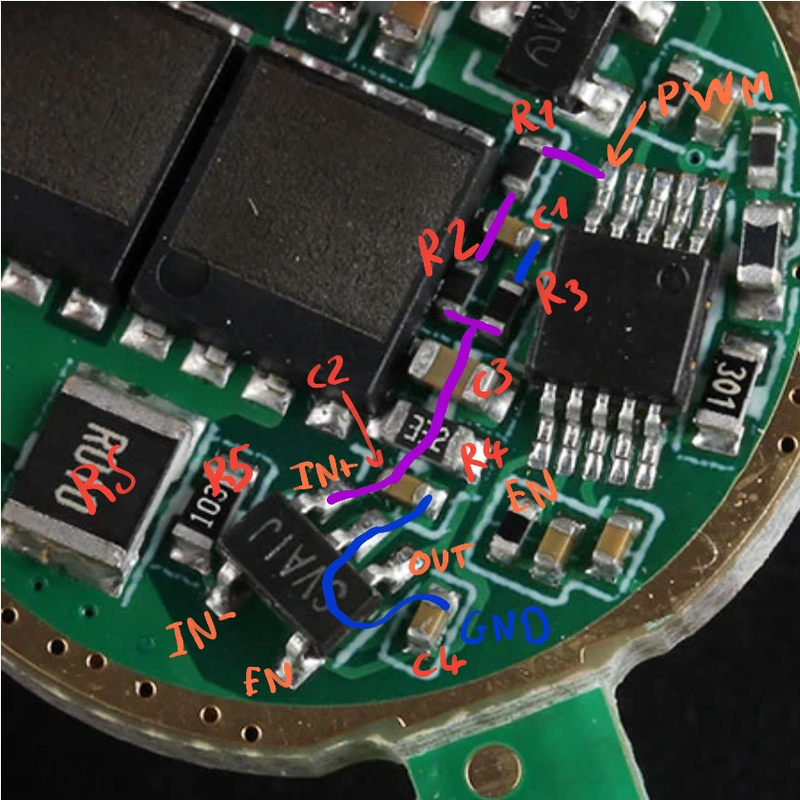
(Not sure if C3 is wired like that but it should be)
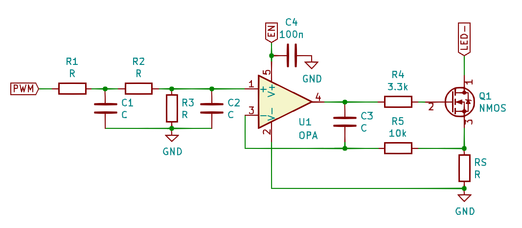
So if you want to change Vsense back to 60mV for a 6A driver (10mΩ Rsense) you would change R2, top resistance of the voltage divider is R2+R1, bottom is R3, R1 and R3 shouldn’t be changed because it will affect the 1st and 2nd RC filter. (Convoy likes to use 2 RC filters, even though it’s not really necessary).
R2 = ((Vreg - Vsense) x R3 / Vsense) - R1
Vreg being the LDO voltage = PWM voltage (measured at 100% output).
Rsense was 1210 size, which was overkill anyway.
2 Thanks
Ah on this one : https://www.aliexpress.com/item/33024197621.html
We can see the resistor values : R1=100k, R2=510K, R3=13k. This would mean Vreg= 2.875 wich is a weird value for an LDO, probably 2.8V and actual Vsense of 58mV for 5.8A.
Assuming they only changed R2 for a Vsense of 120mV the new R2 should be 191k.
edit : there are LDO with 2.85 or 2.9V output, could be one of those too.
1 Thank
I am likely wrong, but would not the 2 stages of RC filters provide a cleaner power path to the MCU and likely increase stability by cleaning up feedback? Also, is there a chance that production changes in the FET may have dictated the change in the sense resistors?
Also above I noted a comment regarding tail cap amps versus LED amps, I would think that based on AWG of the LED wires and quality of the the electrical path that these 2 numbers could differ. Any weakness in the electrical path can affect current flow and would generate some heat in the process. This is why we add spring bypasses, upscale LED wires and do most of the other silly things we do. ![]()
Now, remember I am not a driver engineer, go easy on me if I am wrong!
Matt
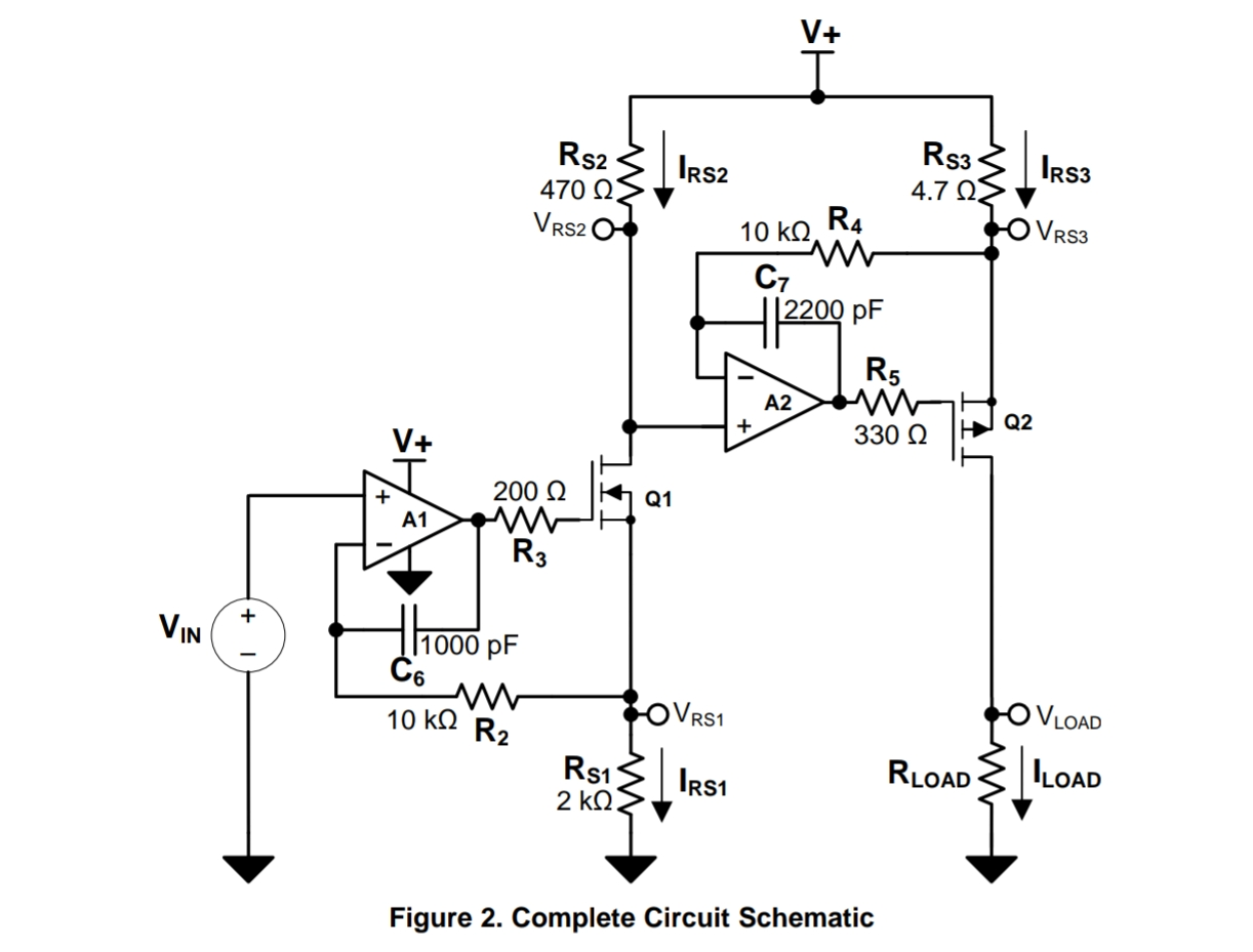
What is the SVA1J ic—is it an op amp? The schematic and pin out traces don’t match.
Typically for a SOT23-5 op amp.
Pin 1 Out
pin 2 Gnd
pin 5 Vcc
Is it a comparator? It looks like the circuit is just using a bang-bang circuit to drive the FET—if PWM is actually a fixed frequency variable duty cycle signal, then the double LPF will remove any of that.
Maybe what is labelled PWM is actually the current limit level?
Yes, 1 is out, then count counter clockwise.
Random datasheet : https://www.mouser.fr/datasheet/2/268/MCP6V96_Family_Data_Sheet_DS20006467A-1948680.pdf
Edit: ah I see what you mean, on the schematic I must have chosen an SC-70 op amp, sorry for the confusion.
There is no feedback coming back to the MCU, it just ouputs a PWM signal, smoothed into a voltage (which sets Vsense) by the RC filters, it just better smooths it with 2 filters and thus reduces the current ripple, but really that’s unnecessary, one is enough, a little ripple is fine, we’re just powering an LED.
For the secong point, it’s a circuit with all the components in series, the current is the same anywhere in the circuit.
If you don’t want any flicker from PWM, then why generate and use it as a command, even with 2 LPFs—just extra stuff not needed.
Just generate a current set point voltage that you want and use the Rsense to feedback the current. Add some compensation or hystersis to prevent high frequency ringing or bang-bang. The setting should be in the command, not the sense resistor. just sayin’
i can’t find any part marked “SVA1” maybe it’s a custom order?
Does C3 connect downstream of the drive resistor R4 between the gate and the source?
ps. Thanks for drawing up the schematic.
That’s what YLP does in the Unicorn 1.0, it lacks precision limited by the ADC’s resolution, and they use an RC filtered PWM signal to drive the mosfet, could be because the MCU doesn’t have a DAC, or because its resolution is not high enough ?
So in the end there is a measurable ripple
It should be across In- and out, quoting an app note I read at some point , with R4 and R5 it forms a compensation network that prevents ringing.
Isn’t not turning the LED blue better? Increased resistance is never ideal but overdriving the LED is rather bad for life expectancy.
Wow! That was fast! I see. O:)
Despite what I said before, the newer version driver will also let a little bit more current if you stack more and more sense resistors, as it reduces the sense voltage burden. The lower modes will grow higher and higher, though, and if you dare to bypass the sense resistor with a blob of solder or by installing copper sheet or wire instead, all modes will top out in output; the lowest one, if set very low by the driver firmware (like 1%), may not (solution: use the most conductive, thickest sense resistor bridge you can afford). In short, you lose modes in this case.
The Convoy “ramping” driver is very solid, really good. Employs a 6788 MOSFET, and just an R005 (5mΩ) sense resistor for up to 8A, so only up to 40mV spent in sense, and the lowest minimum resistance (resistance with the MOSFET “pedal to the metal”, all closed or completely unthrottled) of all linear drivers at Convoy, afaik.
Over time I've learned to appreciate it, despite its weird firmware. It is ideal for gun shooting (hunters), as the mode selection is by series of quick taps: one quick tap, first mode; two quick taps, second mode; three quick taps, third mode. Since the first two modes can be current set with ramping, and the third or special mode can also be set to 100% via the special menu among other options, this means it can be set so that the vibrations of a gun shoot cannot change the output of its flashlight, as all three modes can be easily set equal at 100%.
Here's the sales link of the ∅17/∅22mm ramping driver at Convoy. Oh! :facepalm: I see the chart for the driver mode selection and setting instructions of the driver is missing! Nevermind, the graph is there; it was some sort of connection problem.
Overall I smell a “race for the highest current or output” around here. This is not necessarily a good approach. With the coming of the Osram emitters, with a pretty low Vf and lowest current limits, you need to learn that its drivers must be (or should be) set to limit the maximum current, to avoid any chance of overdriving them. This of course involves looking at the test graphs. However, please bear in mind that not all emitters are equal, and some may have somewhat lower limits. Even if all of them were to stick to no less than the test curves, it is not necessary nor wise to drive them at up to the maximum output current. At these levels, reducing the maximum driving current to let's say ≈80% only renders reliability benefits for the emitter, barely affecting the output. Let's for example see the output graph of a Samsung LH351D 5000K -test- by Texas Ace:

Maximum output current is 9.25A, delivering 2333 lemons.
80% of 9.25 is 7.4, so what do we have at 7.4A? 2220 lemons. This is 2220 / 2333 = 95.15645…% of maximum output at 7.4A, according to test graph information. Do you think this will make a difference to the eye? Go try. x-D
By the way, in the above graph it was easy to see where the maximum output is. Let's take a look at the Reflow conditions tested of Osram KW CSLNM1-KW (White Flat 1mm2) test graph by djozz:

I'll make an small explanation on these duties, just for the sake of it.
So where is the maximum output for these CSLNM1.TG emitters? Is it at 5A? Is it at 6A? Wrong.
djozz only took discrete output measurements each 1A in the latter test (each 0.5A in the former one), and drew straight lines between each discrete value. This is not how the actual output current curve, with continuous measurement or infinite discrete values, looks like.
The actual peak value or maximum in a curve plotted with discrete values and straight lines joining them, is always around the highest discrete value measured for it, and between it and the closest, next highest value. If there are two next highest values, like in the above LH351D curve, then the maximum is spot on the measured point. When there are two maximum discrete values, the peak is between them and higher than both.
In djozz's test the two best emitters peaked a hair above 5.5A, while the lesser performers (excluding the first test's specimen) peaked a little above 5A. In my lightful opinion, I'd probably choose to set my drivers at 4.5A for CSLNM1.TG emitters (the “S” in CSLNM1.TG -1mm²- and CSLPM1.TG -2mm²- means 3030 footprint). There are no tests for the CULNM1.TG or CULPM1.TG ones, so we don't have an idea of the gains for the 4040 footprint. My prediction, though, is that a CULNM1.TG (4040, 1mm²) is barely going to be any better than a CSLNM1.TG (3030, 1mm²). The impact of the footprint may be more noticeable when comparing the CULPM1.TG (4040, 2mm²) to the CSLPM1.TG (3030, 2mm²), but I hardly predict any noticeable gains at stake anyway. Emitter bin is more important in this respect.
Thanks for the technical contributions, thefreeman, it's enlightening. Still, I am @#$% with all of this. I'll see what I do with the sense voltage dividers. I also have a driver from Kaidomain, the P4000, which looked good on paper. But after inspection, I discovered a fairly gross sense resistor stage of an R050 plus 1R0, which is 47.619mΩ, which is efficiency killer for a buck driver driving a 3ish volt load.
P.S.: Now I understand why my latest flashlight build for a brother had such a small brightness difference between the highest mode, and the second highest, as I swapped the sense resistor in its “new downgraded” driver to an R010, like in the older versions of the driver with smaller sense voltage. :facepalm:
I am having a private conversation with Simon right now, this is the last message I just sent him:
I definitely noticed the newer driver with R020 dropping out of regulation quicker compared to an older 17mm 5A driver with R010 and resetting mode group bug in a C8 XP-L HI.
It’s a shame because the 17mm 5A drivers were my go to for modding and Convoy builds, are there other similar alternatives in 17mm besides the LD-A4 and Convoy ramping driver?
Took some time to draw the following picture, peeking at a “new version” (huh?) ∅20mm 12-groups driver, while I was reading the values with my cheap multimeter (maybe gold plated probes can make a difference in this regard) and ensuring all connections were accurate. The SVAKF part is the operational amplifier, LoL. Resistance for R2 would only stick quickly when read with positive probe between it and R3, giving 436.3kΩ. The other way around I get 494.3kΩ after I wait a few seconds for the value to climb up.
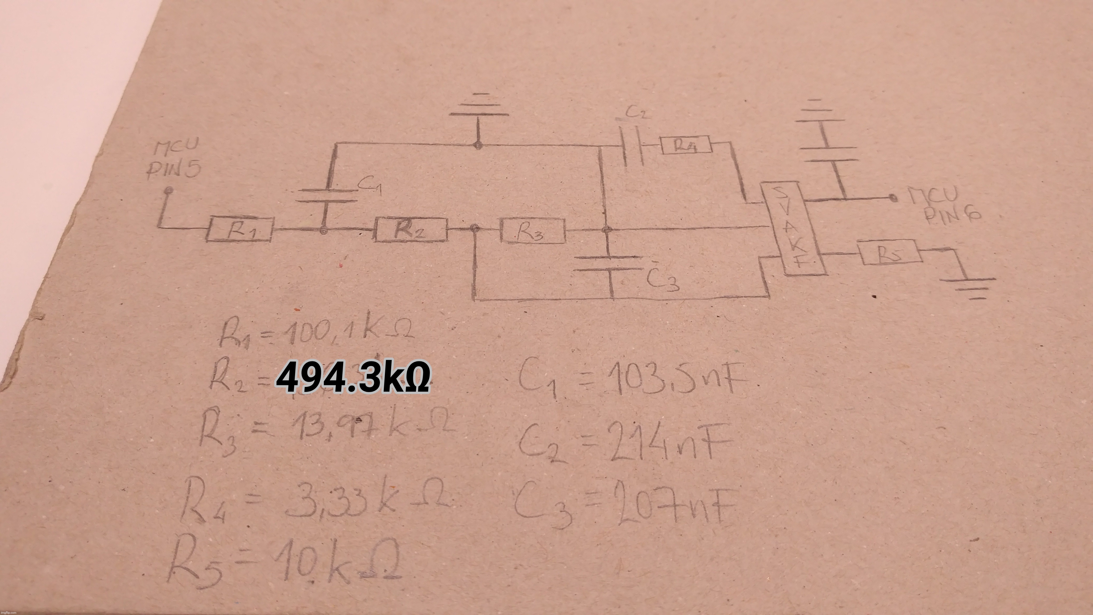
Compared to thefreeman's diagram, C2 <=> C3. I also didn't mess with certain stuff (for example didn't make sure if R5 goes to Rsense first, then to ground).
It's enough for now. O:)
Fri, 08/06/2021 - 16:51
Thanks for that, i was wondering about the capacitor values.
Here is a simulation using the 10mR resistor parameters with your capacitor values running 4A in LED. The ripple in the LED current is due to the low frequency of the “PWM” pulse; if the frequency were increased, then that would be filtered out.

Would you be able to check and provide the actual connection of the R4, R5 and C3 on the output of the op amp to the FET—correct any errors in the schema.
The only difference i can see between the 20mR and 10mR version is the R2 value that you measured, and that difference is not really significant. (436 - 494k vs 510k)
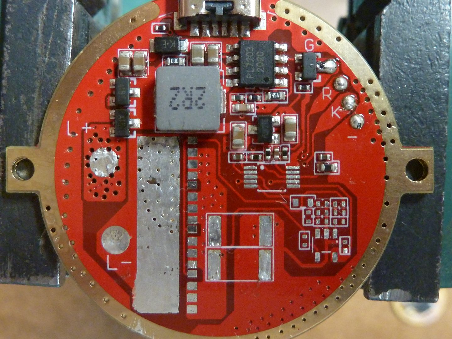
Tom E has a pic of another Convoy linear driver with the components desoldered :
So yeah C3 isn’t between the out and in- contrary to my shematic (I just guessed since it was difficult to see) or shematics found in app notes or even in suggested application in op-amp datasheet , for example this one in the OPA333 DS :
Detailed here : http://www.ti.com/lit/ug/slau502/slau502.pdf
First stage is a constant current sink, the Noctigon kr4 driver is exactly like that, with an added resistor between the gate and source of the mosfet.
Note that with Falstad the circuit is stable even without the compensation capacitor, in LTspice there are large oscillations without it.
It could be that it was intended to be connected for compensation as you have shown, but a trace error was made in the layout. As it is now C3 seems to serve no real purpose or provides any filtering.
If i connect C3 for compensation and increase the command level, now i see 6A in the LED and a 60msec delay in reaching the full drive of the FET with a nice ramp up to the desired current. This sort of soft start puts less wear and tear on the parts and is less abusive than a full hard on start; maybe this was intended but the traces weren’t in place.
[edit]
The op amp will drive the output as necessary to cause the feedback at IN- to match the input at IN. The RC combination of R3*C2 causes an exponential ramp up of the input. With C3 wired as shown it is bleeding off charge from the output thru R5 (10k) to cause IN- to match IN. Once the IN+ reaches its final value and is no longer changing, the contribution by C3 gets reduced and the op amp must drive harder to compensate, which raises the output until it reaches the 1.5V gate threshold voltage of the AO6788 SRFET (30V, 80A, 4mR). Now the FET turns on and the feedback is from the Vsense reading. This is the effect of compensation to create the soft start 60msec delay of current in the LED and FET.
