About Why I start this build
I have been away from the forums for several years since my last LED and driver build. At 2025, I finished my first Fully Constant Current Thrower build named DFEx GT96. Which at that time is the most powerful fully constant current thrower with 62000LM 1700K CD Peak with custom VT LEDs. Here is some picture about this build:


This light uses the first generation of my XTR HyperBoost Fully constant current boost driver that delivering Up to 768 Watts with Up to 97.76% of efficiency to six LEDs. And it has a User Replaceable battery holder to contain six Tab-Less 21700 Battery with 140W PD Fast Charging/discharging capability. Currently this build is fully open-source and every thing to reproduce this light can be found HERE.
From than on, I felt just a thrower isn’t enough. And I wondered if a Flooder that doubles the output from a ACEBEAM X75 and maintain the same four cell form factor is possible. If its possible, that can be the holy grail of my entire flashlight DIY journey. Well, After six months of researching and the answer is Absolutely can. And this post is what I came with.
The Goal of this build
seems this is the last build of my entire flashlight DIY journey, I want it to be as perfect as possible. So here is the goal that I want to Accomplish.
- This light Should be fully regulated at any mode with Full DC Dimming.(means No Direct Drive aka. FET Drive or PWM Chopping)
- This light itself should runs at just four 21700 Cells like original ACEBEAM X75, those cells should be user replaceable without any tools.
- The Battery Holder should have full 140W PD charging/Discharging capability with Smart BMS.
- The Battery Holder should contain full protection(like Reverse/OCP/OVP) and Active Balancing capability to maintain the integrity of the cell at extremely CDR.
- The light should have at least twice amounts of light outputs than ACEBEAM X75 and maintain the intensity as same or a little bit better.
- The light should have ultra low output(eg. 1.0LM Firefly Mode and 200~300LM Moon mode) which ACEBEAM X75 did not have.
The Journey of this build
Design the Battery Holder
For A Build like this, a good starting point is designed the battery holder first. That’s because the size\shape and the contact method of the battery holder will be the origin point for the entire case. Seems the last build(DFEx-GT96)has the same User Replaceable battery holder. That provide a good starting point of battery holder, and I referred to the structure of GT96’s holder than starts the design.
Structural Design For the base of the holder
After setting up all the goals. I starts with the base of the holder and Design everything in Soildworks. here is the finished base with protector.


The base is made of 7075-T6 Aluminum alloy, and being Clamped to Copper nuts(via KM3 Copper screw)on the Protection PCB for both structural support and electrical connection(the surfaces will be machined again to expose the raw aluminum for the negative terminal of the battery subsystem). Also the Protection PCB and the base will be separate by a EPDM material gasket to prevent any possible shorts.
The Center pieces is a huge Brass contact point with gold plating for the positive lead of the battery subsystem. This called “Positive & Negative conductive on the same side” which can accomplish lowest DCR to reduce ohmic loss between the driver and battery subsystem.
Also, you might notice the contacting point for Four cells are sitting at a Separate PCB. That’s because the Cell contact point did not have complex wiring on it. So I use a Double sided Ultra thick copper PCB to minimize the DCR of the trace on PCB. and the Protection PCB uses Four Layer PCB for complex wiring. Here its the Finished Contacting board and Protection PCB:

Electrical Design For the base holder
Consider the crazy amount current which will pass through when turbo mode activated, that means the Protector needs to handle nearly hundreds of Amps without too much temperature rise. So the goal of the protector are listed below:
- The Protector needs to handle Up to 127 Amps for the entire turbo range and the temperature rise should less than 20℃.
- The Protector needs to have a full time balancing feature to maintain the consistency of each cell at every charge/discharge cycle.
- The Protector can handle output short fault and trips to SCP(Short Circuit Protection) Reliably. Without triggering the CID(Current Interruption Device) inside the cell.
- The Protector should have all the protection feature which normal cell protector solution should have. And it can resist to a reverse connected cell at any position without issue.
Considering the size of the PCB and the goal 2, I swap the Main Protect IC to CM1341-FKT from ICM. This IC is a fully integrated Quad Cell Protector perfectly suitable for this use.
Than the Question left is the MOSFET. The MOSFETs needs to be Robust enough to handle extreme current when the output shorted(Typically happened when a catastrophic failure on the driver) and keep cool at turbo. So I chosen the Infineon IQDH29NE2LM5CG for the Main MOSFET. This MOSFET has extreme low RdsON and really high current handle capability.
After A little bit of work, I Finish the design and the schematic looks like this:

The Protecting point of the Protector sets to 125A @ 330mS for OCP1 and 250A @ 33mS for OCP2. This Protection point can trip reliable at short circuit and cuts the power without interrupting the normal operation of the driver. Every cell featuring a BTB PMOS polarity limiter which will stop the current flows into the main portion of the board when the polarity is not right. This ensure the board will not be destroy even the battery is not correctly installed. And here is the finished PCB:


You might notice the back side of the PCB have some orange color things. That’s a reserved solder mask opening for a Thermal Pad between the PCB and the aluminum base. This thermal pad not just for keep the MOSFET/Shunt Resistor cool and transfer the heat to the base. And It also for a second level protection of over-heating.
If the First level thermal protection from driver itself has failed, The heat on the flashlight’s head will accumulate, heats up the base and eventually transfer to the PCB via these thermal pads. When the PCB is hot enough, the Protector will trip and cutting the power to prevent the temperature to rising and causing fire.
Structural Design For the top of the holder
Unlike the battery holder of GT96, I want the battery holder of this build can be easily disassemble and replacing the cells without any tool. Than means I can’t use the old method. So I designed the Top of the holder as a hollow cylinder to contain all the electronic for BMS and charging functions. The Top parts looks like this:

the Bottom Side(aka. the base) Use four Brass Pillar and One Solid Copper Pillar to carry all electrical signal between the top and the base. Also, these Pillars provide structural support to keep these two parts in place. The Function of top Parts Provide extra balancing and smart management for the cell. The BMS contains two PCBs, one is for the actual BMS, the other is for charging subsystem.
And the Top pieces has a solid aluminum panel like this:

This parts provide all the indication light to show the status of battery subsystem as well as a single button to invoke the BMS System. Unlike GT96, This version of BMS did not have a TFT-LCD. That’s because the charge subsystem generate a lots of heat when 140W charging and I need a large surface area as a heat sink to keep it cool. Also, the TFT-LCD will goes bad very quickly at high temperature and become useless.
Electrical Design for BMS/ Active Balancer
Because the extreme Charging/Discharging rate(up to 25C discharge rate & 2C charging rate when using 5000mAh battery) of this build and user can replace the battery, That means the battery will not always have a perfect voltage difference reading(means the consistency is perfect). Sometimes, if the consistency is too bad, just by using the passive balance feature is not enough to fix the consistency problem. So, a much Powerful Energy transfer based Active Balance need to be incorporate to maintain long term stability. The Typical Active Balance method will like this:
- Bi-directional DCDC Based(eg. ETA3000 Series):cheapest, but not stable and can only transfer energy between nearby cells.
- Switching Capacitor Based: Large Current Capability but require more PCB Space for large Capacitor, Also can only transfer energy between nearby cells.
- Push-Pull Transformer Based: Large Current Capability and can transfer energy between any cells. needs a lots of parts with a lots of routing space and requiring expensive transformer.
Considering the cost is not the main factor and this build has four cells, If the balancer can‘t transfer energy between any cell(like Cell1 to Cell4) that means when Balancing, the cells between the unbalanced cells will be over-charged a little to transfer energy, that’s not good. So I used the most complicated solution and fiddling with the layout to fit an entire BMS and Balancer into the first PCB. Here is the schematic and the PCB looks like:


Like the Protector, every cell featuring a BTB PMOS polarity limiter which will stop the current flows into the main portion of the board when the polarity is not right. And the center has a NTC Pad for a film type NTC Resistor to stick into the center of the battery for temperature measurement. And I managed to put a fully functional BMS Analog Front-End(SH367303 from SinoWatt) for both temperature and Cell Voltage measurement. Than the Data will be process by a MCU to provide Advanced BMS Functions. This allow the user to Query overall voltage\consistency\per-cell voltage\worst cell location\temperature from the BMS for health check.
For a typical balancer like this, the driving signal will be generated by a self oscillating gate driver like IR2153STRPBF. but that’s not smart enough for me, so I use software solution which generate these signals via ePWM modules inside the MCU. that means I can adjust the Power level of balancing based on battery status to avoid over-charge the battery(too much current or voltages) or put too much current on the balancer which the balancer can’t handle. And the PWM signal produce by the MCU will be amplify by a UCC27526 dual output gate driver to a proper level which MOSFET feels good.
Also, If the BMS detect the consistency is really bad or the battery is too hot(like just after turbo and the flashlight is super hot), you definitely not want to charge the battery to prevent explosion, So I include some side band via Opto isolator to send command to charging board via FPC. Which can disable charging or reduce charging power as needed to prevent safety hazard. Here its the actual PCB looks like.

Electrical Design for Charger Subsystem
The Charger subsystem is a much easier task by just Providing Type-C input and Output control as well as input detection to wake the BMS up when user inserting a USB cable. For the Type-C Control, I use IP2366 from InjoinIC. This SoC combined an 4-Switch Buck-Boost controller and a USB-C protocol inside the same chip. And I use a simple LMV331 comparator to provide input detection. Here is the PCB and Schematic:


The IP2366 Provided an super easy solution for a Type-C input charging solution with PD3.1 EPR capability. That means this holder can charge four 6000mAh 21700 Cells from 0-100% SOC at constant 28V5A Input for less than 50Minutes of charging time. With Excellent reverse charging capability. Here is all support protocol from this Port for reverse outputs:


The chip not only provide standard PD3.0/3.1 Capability, It also provide Extended PPS/PD3.0 Capability(like 20V7A PD Fix and 6A PPS)for Fast charging of my cell-phone or laptop.
For the Buck-Boost MOSFET, I tried over 20 types of different MOSFETs, and I finally choose the IAUCN07S7L028. Because this MOSFET has the best in class FOMQg( Figure of Merit, low value means much lower switching & conduction loss) in the industry. This means the MOSFET I choose have low conduction and switching losses to improve efficiency. And this Charging solution can archive over 97.4% efficiency during 140W charging. And the top of the PCB looks like this:

The top of the PCB contains the Type-C connector and some LEDs / buttons to indicate the status of the battery and invoke the BMS.
Also, you might notice, the charger PCB did not connect to Battery directly. And I have a ceramic Slow-acting fuse between the Battery and Charger sub-system. This fuse is another safety precautions. If a catastrophe failure occurred in the Charger subsystem, because the much thinner wire between the battery and the charger it will not generating large enough current to trip the protector and the wiring will have large short current flowing through continually and can causing fire easily. So I add this fuse, which will pop as such condition in order to physically cuts the current between battery and the charger permanently.
For why I did not use e-Fuse instead of Traditional fuse, that’s because electronic fuses cannot guarantee reliable interruption of short-circuit currents under such extreme operating conditions every time.
Final Assembly and Machining
After all the design work, its time to export the manufacturing data to supplier and get all the parts for actual holder assembly. This requiring a tons amount of boring ECAD\CAD works.

Here is all the 6061&7075 Aluminum alloy stick for machining. the CNC parts of the Battery Holder is made of 7075-T6 Aluminum for maximum strength.


After a month of waiting, I finally got all the PCBs and Aluminum parts for the holder and its time to assemble it:
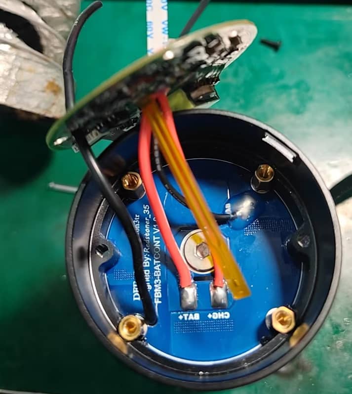


The back side of the Charger board need to be covered by a 0.2mm thickness laser cut mylar sheet for insulation to prevent short circuit. And here its the final ACIR test Result:

The Test battery consists of four TenPower 50XG battery cells with 2.5mΩ of ACIR. That means the DCR or entire holder is just 3.33mΩ(including all contact points and protector PCB) and the ACIR of the battery assembly is only 13.33mΩ in total, Which is crazy value. For comparison, 4 cell version of stock ACEBEAM-X75 lithium battery pack have a typical ACIR of nearly 50mΩ, even the eight cell version have a typical ACIR of 30mΩ.13.33mΩ of ACIR means the battery subsystem in four cell form factor is 60%+ less ACIR than the X75’s battery pack in the same form factor, which means a completely crushing performance.
Design the actual housing
After the holder, its time to starts the design of the actual flashlight housing. The housing design is Co. working by me and a awesome guy named “飘落” in Chinese. For the goal of the design, I want it to be easier to assemble and tough enough for various environment condition. So we came up with a design like this:

To simplify the design, We decide to use the same ID as his own product and modify the case design to adapt the new driver and battery subsystem. The exterior looks like his own Product (name as PL-3,which is a single 49650 battery based flashlight with built-in fans). That means I can re-use the reflector and front cover as well as the front glass panel to save a lots of cost.
Also, You might wondering where the fans are. The fan method is like the GT96, which uses a high speed fan handle DLC, the fan handle has its own battery and switch and can be swap easily. This has a lots of benefits:
- If the fan handle has trouble(like too much noise) you can easily swap it with a new one without any tools required or disassemble the entire flashlight just for fan replacement.
- The Fan handle has its own battery means they won’t steal power from main battery and the light can last much longer.
- The Fan handle has its own driver means the power of the fan can be huge like 36Watts to provide crazy amount of air flow for much better cooling.
Internal Design For Driver thermal management


Due to the extreme output power, even the driver is complete designed by me and have a crazy efficiency, it still generates a lots of heat. So thermal design is a key factor to keep the driver works well. And I designed a carefully shaped driver chamber that have pillars at every heat sources on the driver and conduct the heat directly into the casing.
Handle mount design

The size of this flashlight is very huge, a proper handle mount is critical for user experience. No one will feel comfort when a flashlight equip with a wobbly handle. So for the handle mounting, I referenced the mounting mechanism from ARRI is cinematic camera. with a single UNC1/4 screws in middle to provide vertical stress handling. And I add two locating pins combined with the horizontal bar to provide horizontal and roll limits. This creates a robust mounting solution for handle.
Button / Front ring Machining
For save costs, the Button assembly is a standard parts from DDH(“东东海” in Chinese) And looks like this:

This button assembly looks OK, but the material is SUS304, which is too soft for a things that will be touch by people every day. So I use a table-top polisher with cotton wheel, combined with polishing paste to polish it into mirror finish. And I do the same treatment to the front ring of the flashlight. Than I will sent the parts to DLC coating supplier and coat them with DLC(Diamond Like Carbon) coating.



By the way, the entire polishing process is a completely nightmare, My entire body and my face is completely covered by black gunk with really bad smell  . I took several hours to get rid of all gunk away from my body by a deep wash. but the result is good.
After the nightmare of polishing, the next things is to ship the part to PVD coating lab, to do the DLC Coating. here is the finished result:


After the DLC Coating, the color of the parts will turns to a beautiful looking gray. That coating not only give the parts a perfect exterior, it also improve the hardness a lot. After DLC, the surface hardness will bump to 5000HV or more, which makes the surface of these parts as hard as diamond. This means daily used object(eg. keys or screw driver) is not possible to scratch the surface and leaving visible marks.
Machining and Post processing for the housing
Although the front ring of this flashlight can reuse existing parts, the body and head are newly designed, so five-axis CNC machining is required. And I sent the CAD files to supplier and wait for them the finish machining as well as Type-III hard Anodizing.


Considering durability, unlike the last run of GT96, this time I only made a black hard anodized version instead of colorful anodized one. It may not look as flashy as before, but the durability is greatly improved. After all the machining process done, the last step is Selective Chemical etching to precisely remove the anodized layer at a specific spot to achieve better conductivity and heat transfer.


Design the driver
Due to the design goal of the driver(Stays cool\high efficiency at turbo mode and remain regulation at any mode including the turbo mode). That means a cheating solution previously used in high output flashlight (eg. Small current Buck for lower gear and a direct drive MOSFET to connect battery into LED directly for turbo mode) is not acceptable. To accomplish the goal, I need to make a High power DC-DC converter that can deliver at least 1.1KW into the LED to achieve the initial project goal regarding the lumen value. Also, the DC-DC converter should have decent efficiency at light load in order to make the lower gear of the flashlight last longer.
After implementing the above requirements, this DCDC converter and the circuit required to achieve such a wide output range still need to be fitted into a driver PCB with size similar to the X75, which means nearly doubled power density. At first, it seems impossible. But As I said earlier,Nothing is impossible with amazing engineering & enough money. So I came up with industry’s first Low Voltage Enhancement-mode Gallium Nitride Field-Effect Transistor(LV-eGaN FET) Based driver And accomplish all goals that I setup.
Select the topology
When talks to Fully Constant Current DC-DC Based Driver, people typically will use BUCK topology and keep the LED’s working voltages less than half of battery voltage. Or use boost topology and keep the LED’s working voltages at twice amount of battery. Here is the actual calculation of each topology:
- BUCK: 4S Lithium Input to drive 6V LEDs. If desired output power is 1150Watt and the LED Voltage is 6.4V(3.2V per Chip), that means the Driver needs to put 1150/6.4=179.6875 Amps of current into the LED.
- BOOST: 4S Lithium Input to drive 24V LEDs. If desired output power is 1150Watt and the LED Voltage is 25.6V(3.2V per Chip), that means the Driver needs to put 1150/(25.6)=44.92 Amps of current into the LED.
Considering that Ohmic losses increase exponentially with current, this means that using a BUCK scheme to output 179A to a 6V LED is almost impossible. Forcing this would result in enormous conduction losses means the driver will easily overheat and become unstable. So the only solution is using a Dual phase interleaving boost controller like the LTC3787 in my last build.
Fighting with Ploss(early design stages)
To archive that much amount of Output Power, just using 3S Battery like my last build is too less. So I moved to 4S Platform for much more voltages and larger power. This brings us to our first problem. A 30V rated MOSFET works fine in a 3S application, but clearly it’s not enough for the minimum 33V open-circuit voltage required by a 24V LED. So I need to use a 60V MOSFET. So I decide to use ONSEMI’s source down Silicon MOSFETs for control FET and drive with a external gate drive. and to Top Sync FET is a DSC MOSFETs. And that’s the original Sample PCB:

This driver is basically a modified version of GT96’s driver. It uses the same LTC3787 Boost controller, but swap the PAD of MOSFETs for higher voltage rating. And it incorporate an AUX Power-Supply to provide 5V for Driving the Sync. MOSFET. After a little bit of time, I test it with a SFY55 LED. Then I was immediately disappointed with the result when I starts it. Not only it consumes too much power at low gear, it also screaming like crazy. When I hook the oscilloscope to the switching node, I got this 

The control loop is completely ****ed up and oscillate like crazy. after a little bit of Comp adjustment, it looks like its stable, but the bottom FET is hot, so hot that I even not dare to run it at turbo. At first, I think the problem is causing by insufficient dead time and the current is shooting through the TOP & Bottom FET, so I removed the Top MOSFET and soldering a Diode to see if any improvement happens.

After soldering, I hook it up again to the bench, and nothing changes. At this time, I was already in despair. I could not determine where this wasted energy had gone. Given such heat performance, I did not have the courage to operate the driver at full power(Turbo mode). That situation makes me wonder, Is it really impossible to build a 1.2KW DC-DC with great light load efficiency in this limited space?
Moving to Gallium Nitride
From the early failed tries on Silicon, that means this problem is not a easy task to solve. Try to use the existing Silicon based solution is a dead end. At this time, I was already in despair. So I decide to have a rest and maybe get some other solution by accident.
One day, I decide to do some randomly search on ADI’s website to see if using Gallium Nitride is possible. than I saw this:

When I saw this component, I felt it was the golden key to solving the problem. This new component is essentially the same as the LTC3787 used in the previous silicon-based solution in terms of loop compensation and peripheral design. This means I can migrate from silicon MOSFETs to gallium nitride with a very small cost, achieving what was previously impossible. After confirming with the component distributor that the part was in stock, I immediately downloaded LTPowerCAD and did some initial simulations:


From the simulation results, you can see that the new gallium nitride solution is much more efficient, especially under light loads. This is because gallium nitride’s extremely low switching charge and zero reverse recovery characteristics greatly reduce switching losses. This means I can increase the switching frequency from 340KHz in the silicon-based solution to 460KHz, allowing the use of inductors with smaller inductance and higher saturation current, further boosting the drive’s output capability and efficiency.
Some Basic Calculation
After determining the system’s switching frequency, the next step is to calculate the fundamental parameters of the system’s inductor, current sensing method, and current sense resistor based on the device manual. Based on the equation in the LTC7892’s document:
∆IL = 1/(f •L) •VIN • (1 − VIN/VOUT)
With the output voltage parameters and ∆IL known, a rearranged version of this formula can be used to back-calculate the inductor value suitable for the operating conditions. Based on an input of 14.4V, an output of about 26V, an output current of about 45A, and ΔIL around 40%, I chose theXAL1580-102inductor. And I calculate the maximum possible average current inside the inductor at VinD(which is the situation for maximum input current) by the equation in the LTC7892’s document:
IL(MAX) = IOUT(MAX) • VOUT/VIN.
For a driver with four-cell lithium battery input, under extreme load, the input voltage will drop close to the battery’s nominal voltage. So I take 14.4V as the VIN. At this time, the average inductor current will be 45*26/14.4=81.25A. Since the driver operates in two-phase interleaving, it has two phases. Moreover, during the design, I used a 40% ΔIL coefficient. Therefore, the peak inductor current for each phase can be calculated using the following formula:
IL(Peak per Phase ) = ((1+ΔIL Coff./2)*(ILMax Total./2) = ((81.25/2)*1.20) = 48.75A
The inductor I chosen ( XAL1580-102 ) has a saturation current of 73.5A, that means we have enough headroom to avoid saturation. And the next two things that I need to decide is the current sensing method. Generally speaking, for this type of boost converter, there are the following two optional current sensing schemes:
- Large Sensing Resistor with low ohms
- Use Inductor DCR sensing (Using the parasitic DC resistance of an inductor to replace large and heat-generating low-value resistors)
Although using DCR detection can save the PCB space occupied by the shunt resistor(No heat and losses from them) and improve efficiency, the DCR method has two fatal shortcomings:
- The sensing method requiring perfect matching between RC coefficient of your sample filter & inductor’s DCR and inductance.
- The accuracy of this method relies heavily on the DCR of the inductor.
First of all, an accurate overcurrent protection function is crucial for drivers using Gallium Nitride (GaN) FETs (GaN has poorer surge tolerance, which means it cannot withstand the massive current surges caused by inductor saturation for a short period of time as silicon-based MOSFETs can). For inductor manufacturers, DCR is a parasitic parameter guaranteed only by design and is not specifically controlled like resistance to ensure consistency with the nominal value. This means that overcurrent protection provided by this method is extremely inaccurate with huge thermal drift.
Based on the above reasons, I use sensing Large Resistor based Current sensing to provide perfect OCP accuracy(up to ±1%) with the cost of a little more heat. The next things is calculate the resistor value and select packaging based on the equation in the LTC7892 datasheet:
RSENSE = VSENSE(MAX)/(IL(MAX)+∆IL/2)
The latter part of this equation represents the peak current of the inductor, which has already been solved above. As for Vsensemax, based on the hardware configuration, I chose 50 mV, so the required resistance value can be easily calculated:
RSENSE = 50mV / 48.75A = 1.025mΩ
Although the result calculated from the equation is just enough, considering the voltage drop of the battery, if this value happens to be at the critical threshold, it could cause the inductor current to be clamped at the maximum allowable peak at low battery voltage, resulting in the output current failing to reach the target value. This means that the driver would exit the constant current mode, which is unacceptable to me. Therefore, I chose a 0.75 mΩ resistor. This means the Peak current limit will be set to:
ILpeak(Max) = 50mV / 0.75mΩ = 66.67A
This value precisely allows the FET and the inductor to withstand it (the inductor’s saturation current is 73.5 A) and provides sufficient margin to ensure that the driver can maintain a constant current output under any condition without being constrained by input current limitations. The final step is to calculate the RC filter between the input current sense resistor and the chip. This is a extremely important step according to the instruction in the manual:
The parasitic inductance (ESL) of the sense resistor introduces significant error in the current sense signal for lower
inductor value (<3μH) or higher current (>5A) applications. This error is proportional to the input voltage and can
degrade line regulation or cause loop instability. Placing an RC filter (filter resistor, RF and filter capacitor, CF) into the
SENSEx+ and SENSEx− pins.
According to the initial test and some basic equation in the datasheet, I decide to to use Rf = 51Ω, Cf = 6.8nF to construct the RC Filter. This filter has a Crossover Frequency(Fc,-3db) of 460KHz and 793KHz of -6db cutoff frequency. The cutoff frequency of this filter happens to be close to the switching frequency of the DC-DC, which means that error signals introduced by the resistor’s ESL will be blocked and will not affect the normal inductor peak current signal at the resistor equal to the switching frequency.
Complete the layout and for the first try
After completing the simulation, the next step is the actual layout and routing, converting the design into a usable circuit board. This is quite a challenging task, as the new LTC7892 chip has increased significantly in size from the original 5x4 mm to 6x6 mm, which means that sophisticated layout and routing techniques are required to fit all the components while maintaining the same driver form factor. And Also, I need to decide which brand of GaN FET is suitable for this task. Currently, there are only three manufacturers worldwide that can produce low-voltage enhanced gallium nitride devices:
- InnoScience
- Infineon (technology sourced from the acquisition of GaN Systems Inc.)
- EPC
Although EPC’s gallium nitride has the industry’s top performance, I was stunned when I opened the device datasheet and saw the package diagram:

This type of package is called FCQFN. For planar devices, it can achieve the lowest package parasitic parameters, but this means that a special PCB with multiple copper layers and many vias is required to achieve sufficient current carrying capacity. Considering that the inner layers of this PCB are already completely filled and there is not enough space to implement current conduction, I then looked at Innoscience’s gallium nitride and its packaging is something like this:

Their devices adopt PDFN33/PDFN56 packages that are downward compatible with silicon MOSFETs, which means the layout and routing will be much simpler. After a whole day of repeatedly struggling with the layout and routing, I finally completed the initial design of the GaN driver. Next comes the most exciting time: PCB fabrication, soldering, and power-on testing.

This test is a completely different story. This time when powered on, the drive behaved like a well-behaved child, without any serious abnormalities, and the issue of abnormally high temperature under light load has been greatly alleviated. I finally dared to run the drive at full load at the rated power corresponding to the ECO maximum brightness setting, and the test results are pleasing:

The driver remains completely stable under this load condition with no audible buzzing. At the same time, the driver efficiency is surprisingly high, with a measured board-end voltage showing an operational efficiency of up to 97.7%. This means the gallium nitride solution is totally feasible!

This is the switch node voltage waveform measured while the driver is operating. The waveform is very stable, with no severe overshoot. There are only slight steps caused by the dead time at the end of the rising edge and the beginning of the falling edge. This indicates that the parasitic parameters of this layout are very ideal.
Finalized the Driver
After the initial testing and debugging of the engineering prototype, the gallium nitride driver is finally ready for practical use. At this point, I completed the final optimisation of the schematic, and the following is the final schematic:

You might notice the FB portion is much different than any other driver in the market. that’s because I use a special output modulation method consist of both Constant Voltage/Constant Current Servo loops. combined with a high slew rate path MOSFET, this driver can archive 16Hz high speed strobe at 1.15KW full power without having to sacrifice the slope of strobe mode. And the voltage servo loop allow me to extend the DC-dimming range all the way down to 1LM to accomplish the firefly mode in the goal of this build.
In the final version, to achieve low power consumption, I designed a highly sophisticated power distribution network. This network, combined with the power and output state management state machine in the firmware, optimizes the power distribution across the entire system, significantly reducing power consumption compared to the X75 driver. This allows the driver to reduce its own power consumption to an extremely low level at very low output power, thereby making the endurance at ultra-low brightness levels truly usable.
In addition, consistent with the driver used by the GT96, this driver’s hardware and software feature highly complex self-test and protection mechanisms. During every power-up and operation, the driver checks its own status and load conditions to prevent more serious accidents caused by its own hardware failures. Here is the final version of the driver:

And here is the Waveform of the Switching node of the finalized driver:


The Rising edge is perfect without any ringing. This indicates that the final version of the driver has no issues with the layout and wiring. The rising edge of the SW node exhibits only a single spike caused by freewheeling of the inductor through the FET channel during the dead time. After extending the timing base, the overall waveform remains extremely stable, indicating that the current sampling and loop compensation of the driver are at an optimal level. According to actual measurements, the final version of the driver can achieve a board-end efficiency of 97.81% in the Turbo mode, which means that in this mode, the driver generates less heat, allowing more thermal capacity for the LED’s waste heat.
Design the LED & MCPCB
To save costs, I used off-the-shelf light cup components during the housing design phase. However, this led to a serious issue. The standard light cup components include mounting positions for ten LEDs. The driver only accepts 24V LEDs, which means that neither 3V nor 6V LEDs can achieve the required voltage for the driver. Therefore, I had to customize dedicated 12V LEDs to achieve 24V in a 2S5P configuration.
LED
Seems the LED needs to be 12V of working voltage, that means the number of LED chips Must be divisible by 4. and I want a Square LES. so the possible chip count is 16 Chips. due to the amount of chips can be installed, smaller chips did not have enough current handling capability to handle that much of current, That’s why I decide to use larger chips like SANAN S-55CBFSD-E. This is the latest generation of SANAN’s 55mil size Flip-Chip LED which undergone sufficient market testing. This chip has good optical efficiency and moderate voltage and light density, making it suitable for driving with a constant current method.
Although SANAN Optoelectronics has launched its latest 55mil chip (named 55F), considering that this chip has not yet undergone sufficient market testing, I did not choose to use it.
After determining which LED chip to use, the next step is complete the 3D Modeling based on official datasheet from chip fab and process capability of the packaging fab like this:


This 3D Modeling is based on the size parameter of the LED Chip, And I complete everything including the trace design of AIN substrate and Solder Pad. Seems this is a completely custom LED, I use a private 8080(8*8mm) form factor. This Form factor can offer much larger thermal pad for much better thermal performance.
After determining the package form factor and chip arrangement, its important to calculate how much current for each chip and to avoid put too much current on them(When SANAN’s large-size chips operate under over-drive conditions, they experience quite serious reliability issues. The chips become fragile and are prone to cracking or exhibiting abnormal electrical parameters).here is the calculation result:
- Maximum rated current of each chip : 3000mA
- Equivalent chips connected in parallel inside each LED package: 4S4P means 4chips in parallel.
- Maximum Current for Each Package : 3000(mA)x4(Chips)=12000mA=12A
- Equivalent LED Package connected in parallel inside each MCPCB: 2S5P means 5 LED Packages in parallel.
- Maximum Current for Entire MCPCB : 12000(mA)x5(Packages)=60000mA=60A.
The maximum output power which driver capable is 45000mA aka. 45Amps, and the MCPCB can handle 60Amps and even more for overdriving. That means the LED is driving below its rated operating point and we have 15Amps of reserved headroom. Driving the LED below the rating current not only extend the life of the chip, and it improves lumen efficiency.
The final step is to sent the data to packaging fab and make the LED. They will transfer the 3D modeling into the actual drawings for the AIN substrate and other things:

After a month, I receive the LED in a small packaging and its ready to soldered them to the MCPCB.

And this is the Test Report produce by the LED Fab:

For this LED, I choose Neutral White CCT which is 5000-5500K range for higher lumen efficiency. At binning condition, the CCT will located at 5250-5300K. And I use a new fluorescent powder formula as well as coating method which inspired by NightWatch’s LED. This type of fluorescent powder can product extremely high lumen efficiency without annoying greenish tint like Luminus or CREE XHP 70.2 LED will produce.
MCPCB
The MCPCB Design is pretty straight forward. Once the LED design is complete, I just complete the design in ECAD software. Here is the 2D and 3D view of the MCPCB.

Although the use of a high voltage design means that the MCPCB only needs to withstand around 40 amperes of current, I still used an MCPCB with a thickness of 3mm and 6Oz copper layer to minimize losses. The 3mm thickness ensures sufficient thermal capacity and lateral heat conduction paths to dissipate the substantial heat generated by the LEDs.

After the MCPCB Arrives, here is the final look of MCPCB with LED on it. Also, you should notice that there is a Schottky diode connected in reverse across the positive and negative terminals of the MCPCB. This diode helps release the reverse high voltage generated by the parasitic inductance in the LEDs and the substrate packaging during high-frequency strobe, protecting the path MOSFET.
Final Assembly
After 5 Months of waiting, its time to put everything together!

Chemically polish and passivate the drive retainer ring


Install the driver

Install the MCPCB


install the reflector & front glass at Ultra clean bench.

Done!
Exterior Look and Weight


The final product’s dimensions are quite reasonable for the size of my hand, but considering its considerable weight, I would still prefer to use the accompanying fan handle as a handheld lamp.


here is the weight of the build(/w and/wo Fan handle DLC):


- Weight without fan handle: 2068.1G
- Weight with fan handle: 2355.9G
The weight of the finished product does indeed slightly exceed my expectations. However, considering such an extraordinary output power and brightness, the additional weight brings thermal capacity that can better extend the duration of Turbo mode output.
Beam Profile


The beam profile is a hybrid between flooder and a thrower. which is the type of beam profile that I want. I apologize for the severe overexposure in the images of the beam pattern. Due to the extreme brightness output of this flashlight far exceeding the capabilities of my phone’s camera, the images are severely overexposed regardless of how I adjust the shooting settings.
Performance Graph
After tons of work, its time to see if the performance reaches the goal of this project. here is the Realtime Lumen graph of cycle mode and
Turbo mode. Considering the extravagant use of materials and cost, such performance is to be expected. Here is the runtime summary of this build.

Turbo Mode(Including Power & ECO)

For safety reason, the firmware have two different Turbo mode profile with different Lumens and thermal control profile. And the driver has battery discharge capability detection. If the Input MPPT detected the battery is too weak for Power Mode, It will automatically adapts to poor battery. The input MPPT algorithm will detect how much current the battery can produce, and the amounts of power using by turbo mode will be limited to the maximum capabilities of the poor battery. This means the driver will not over-drained the battery by sucking too much current(which might destroy the battery). At this time, the driver will switch to ECO mode and alerts the user by display a light sequence at the key.
The Power mode has the highest output which up to 153600LM and 520K Candlelight of intensity and remains for nearly 45000LM for 9minutes(cooling by the Fan DLC with 36Watts of fan power).Which is absolutely crazy.
And the ECO mode with less lumen which tops out at 97500LM and can sustain regulation for nearly two minutes!
Normal Mode

For the normal gear levels, this is truly where gallium nitride (GaN) drivers can showcase their ultimate performance. Due to the extremely high efficiency of GaN drivers and the boost constant current topology, when using a fan handle for cooling, nearly linear lumen maintenance can be achieved at each gear level, without linear decline as battery level decreases. At the same time, to achieve the longest runtime, this UI system employs sequential step-downs to maximize battery utilization. This is also why the curves exhibit multiple steps.
Charging Capability
Considering the flashlight’s enormous output power, frequent recharging of the battery is certainly necessary. Therefore, the flashlight’s fast charging capability is crucial for the user experience. Below is the charging curve of the flashlight using a 140W PD charger from 0% SoC to full charge after discharge.
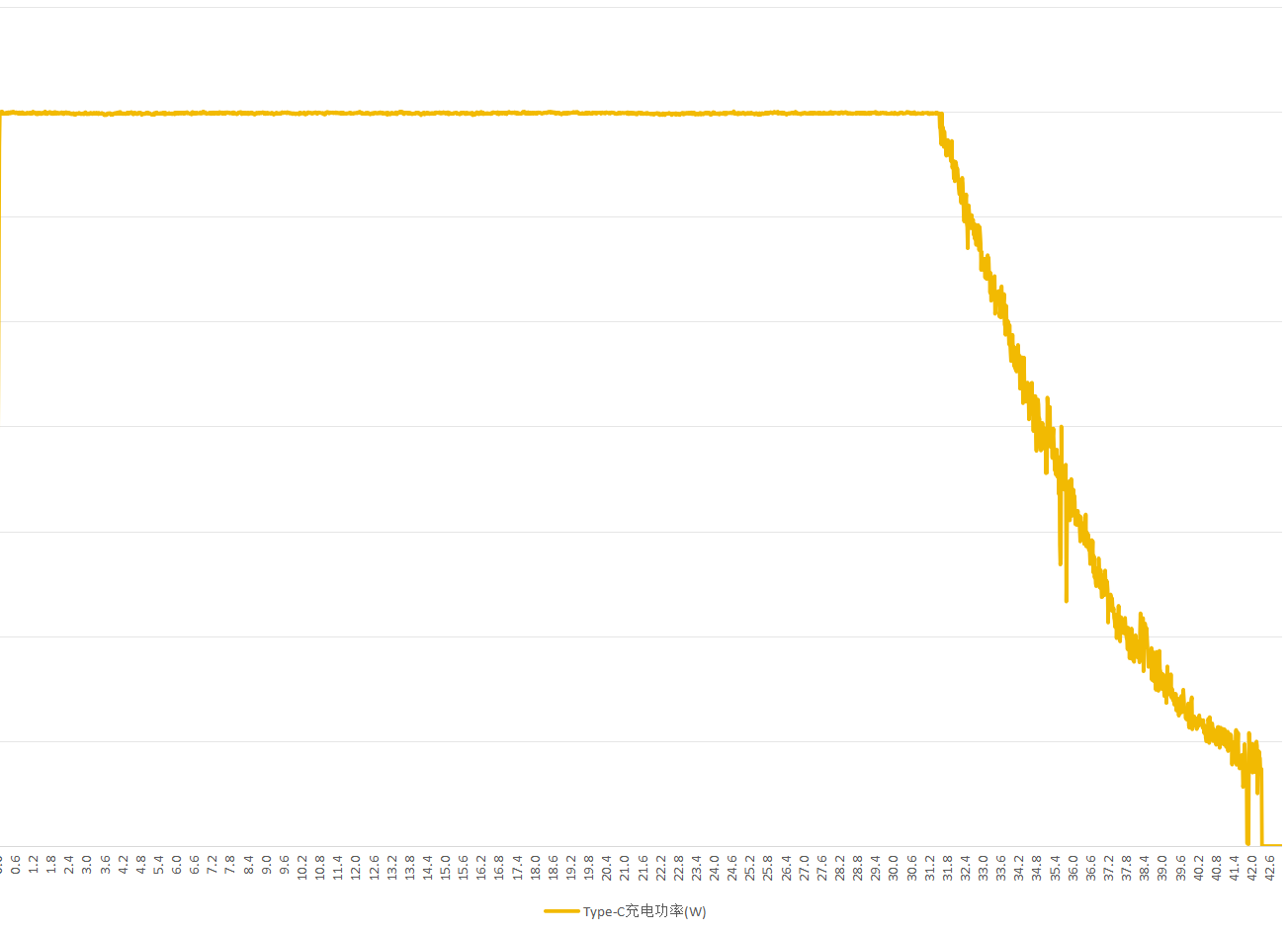
Before 32 minutes and 19 seconds, the flashlight maintained a constant current charging of the battery at an input power of up to 140W, charging the majority of the battery. Then the torch switched to constant voltage charging mode, with the charging power gradually decreasing until it reached zero at 42 minutes and 16 seconds, completing the entire charging process. This means that even if the battery is depleted, users can immediately restore the torch to full power within an hour, and with the addition of a replaceable battery mechanism, the user experience is greatly enhanced.
Output voltage Ripple(For Power bank function)
From the outset of its design, this flashlight is equipped with a mobile power bank function capable of a maximum output of 140W. This allows users to quickly charge devices such as flashlights or laptops outdoors. Additionally, users can take advantage of the flashlight’s replaceable battery feature to make use of a large number of idle 21700 batteries. Therefore, the quality of the output from this power bank is crucial. The following shows the measured output ripple under full load at 140W

Output ripple at PD3.0 140W.

Output ripple at PD3.1 140W @ 28V 5A.
It can be seen that the power bank function of this flashlight delivers excellent output quality. Even under the heavy load of 140W at full capacity, it can maintain an extremely low output ripple of 6mVpp. For reference, typical PD chargers usually have an output ripple of at least 50 to 100mVpp when fully loaded.
Some ramblings and afterwords…
This project was initiated in April this year and lasted for nearly five months. All electronic components, the overall structure and circuit design of the battery rack, part of the casing design, complete performance and endurance testing, as well as the design of the optoelectronic components and coordination with relevant suppliers were independently completed by the author (redstoner_35). During this process, I received both financial and moral support from several important friends and my family, helping me when I was on the verge of giving up. I am very grateful to @KIPA, @思绪 and my family for their moral and financial support, as well as to 飘落396 for support in CNC and casing structure design. This support has been a crucial force in ensuring the continuation and eventual success of this project.
As a DIY enthusiast, I have always sought to inspire high-quality top-tier solutions to come to fruition. Therefore, after organizing all the materials, all production resources for this project (including the hardware for the casing and electronics, as well as the complete program source code for all the firmware) will be open-sourced on GitHub. Please look forward to it.
Github Repos(AUG 21 2026 Updated)
After a lots of work, I finally managed to prepare everything of this project and push them to the github. HERE is the link to the repo of this project. Enjoy  !