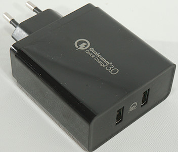
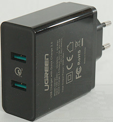
UGreen QC3 charger 36W CD161
Official specifications:
-
Brand Ugreen
-
Model No: CD161
-
Input: 100-240VAC 50/60Hz
-
Output power: 36W max.
-
Output each connector: 5V 3A, 9V 2A, 12V 1.5A
-
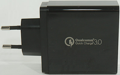
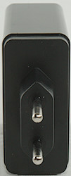
Size: 68mm x 63mm x 29mm
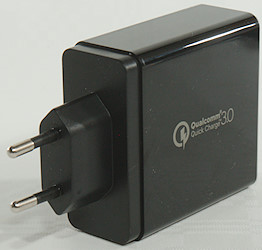
I got it from aliexpress dealer: Ugreen Official Store
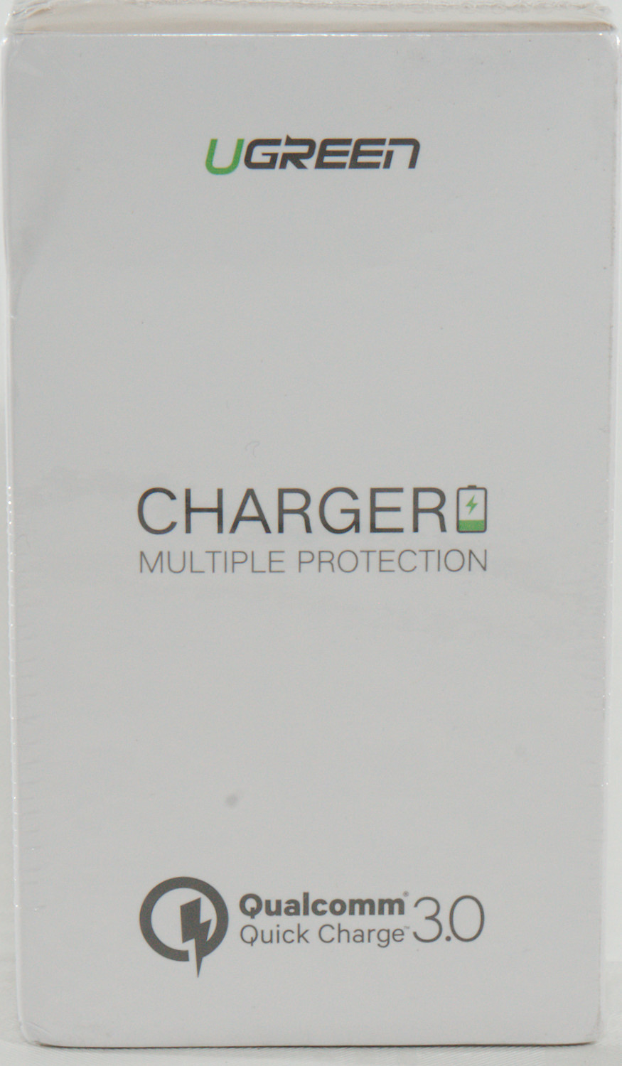

i got it in a white cardboard box.
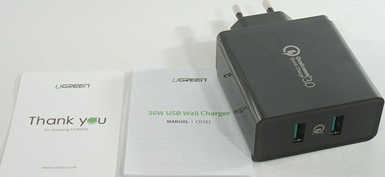
It contained the charger and a instruction sheet.

Measurements
-
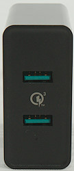
USB outputs are coded as Apple 2.4A, DCP, QC3, Samsung-AFC, Huawei-FCP
-
Minimum QC3 voltage is 3.7V
-
Power consumption when idle is 0.18 Watt
-
Weight: 149g
-
Size: 104.4 x 63.2 29.2mm
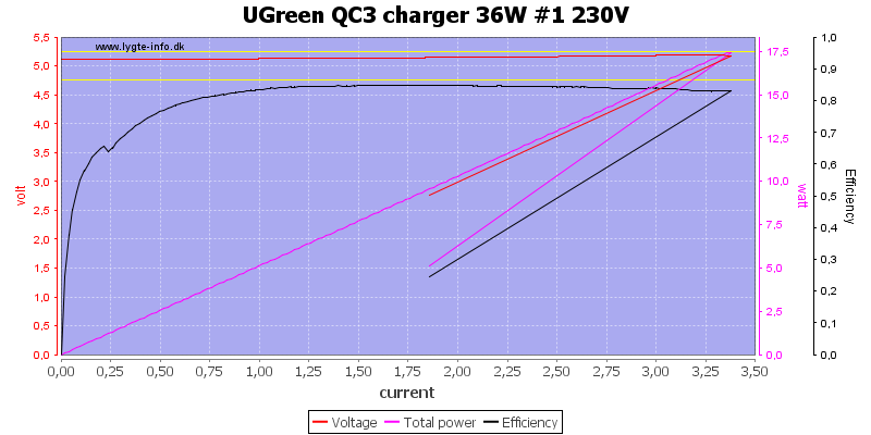
The 3A QC output can deliver about 3.3A with cable compensation, this is fine.
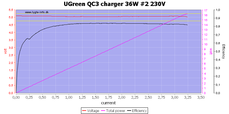
The other output is similar.
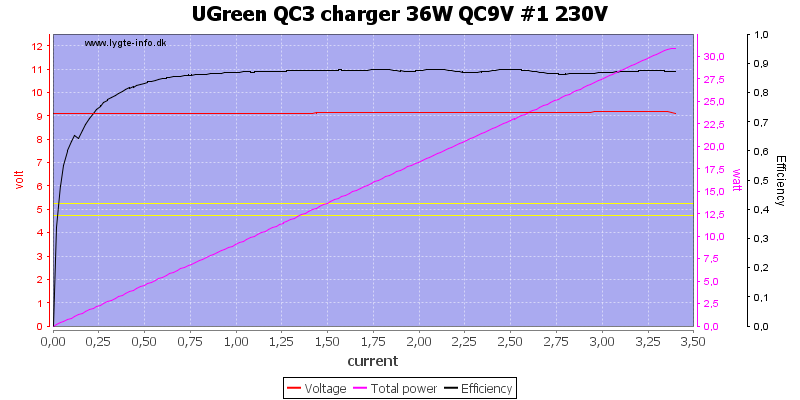
At 9V the output current is still 3.3A
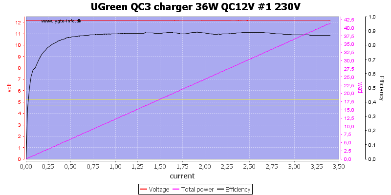
And even at 12V it maintains the 3.3V maximum output current.
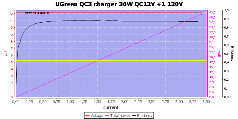
And also at 120VAC.
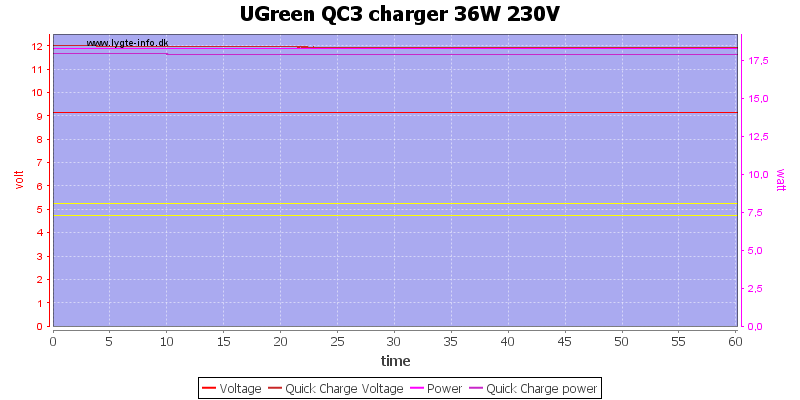
For a load test I used 9V 2A and 12V 1.5A for one hour, it worked fine (Both outputs are QC, but I did not change standard my labels on the chart).
The temperature photos below are taken between 30 minutes and 60 minutes into the one hour test.
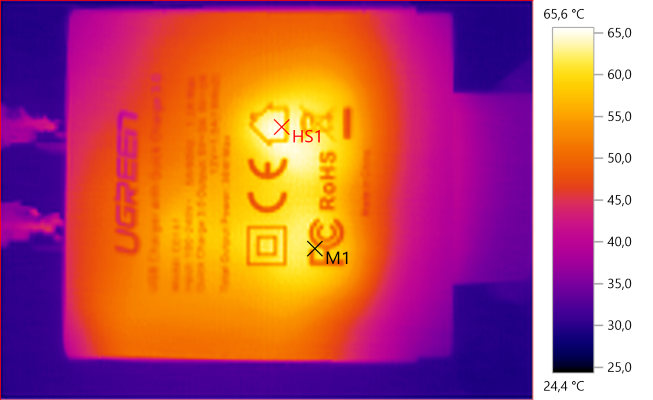
M1: 59.5°C, HS1: 65.6°C
HS1 is the transformer.
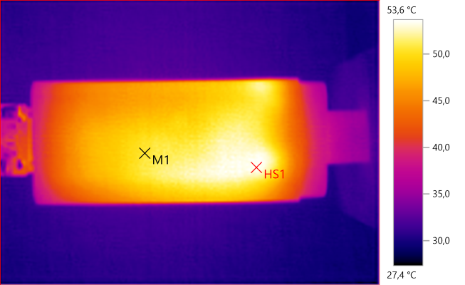
M1: 50.5°C, HS1: 53.6°C
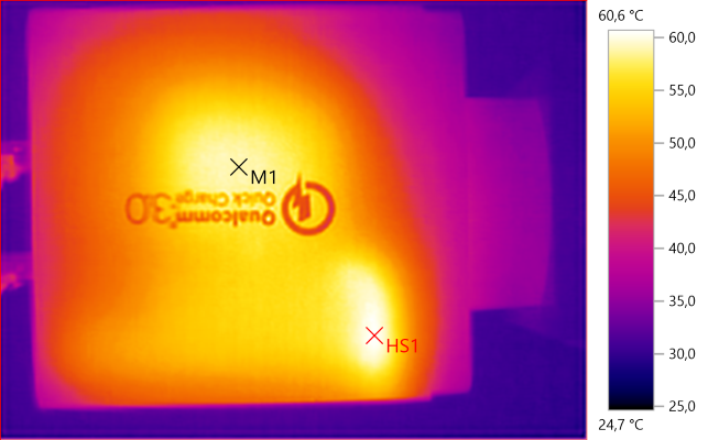
M1: 58.9°C, HS1: 60.6°C
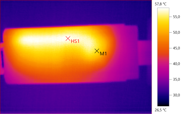
M1: 53.6°C, HS1: 57.8°C
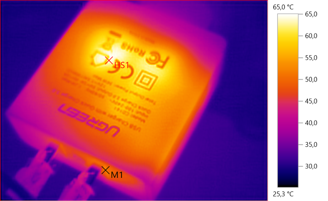
M1: 51.9°C, HS1: 65.0°C
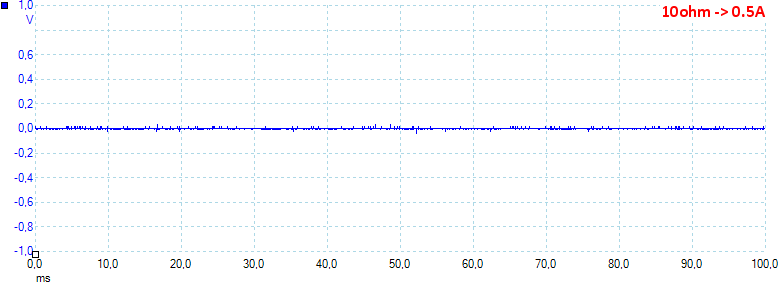
At 0.5A the noise is 4mV rms and 77mVpp.
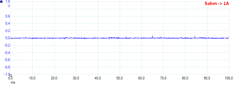
At 1A the noise is 4mV rms and 137mVpp.
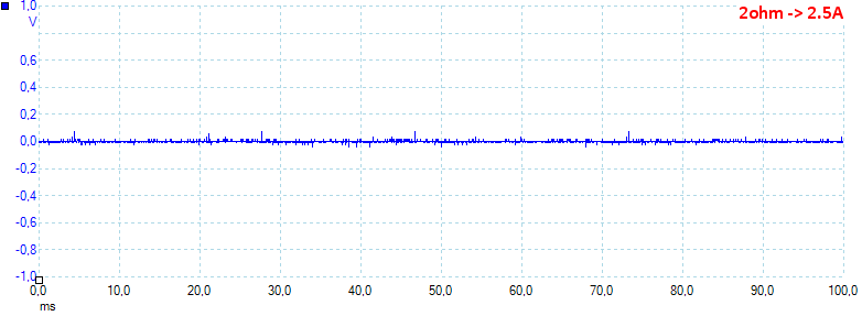
At 2.5A the noise is 6mV rms and 147mVpp.
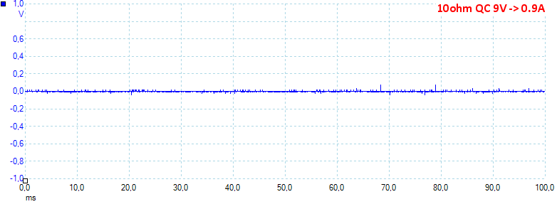
At 9V 0.9A the noise is 5mV rms and 130mVpp.
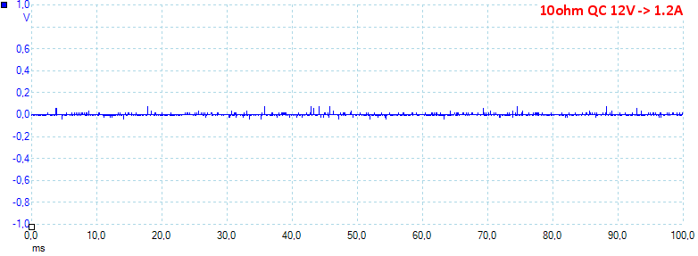
At 12V 1.2A the noise is 5mV rms and 143mVpp, all very low values.
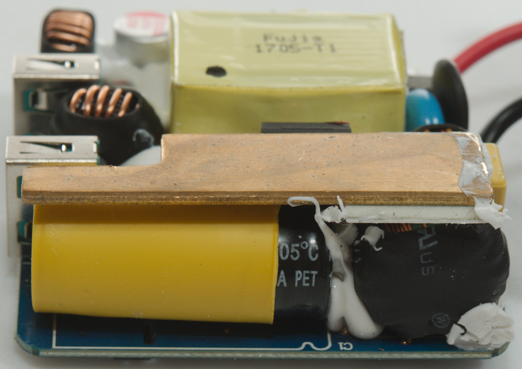
Tear down
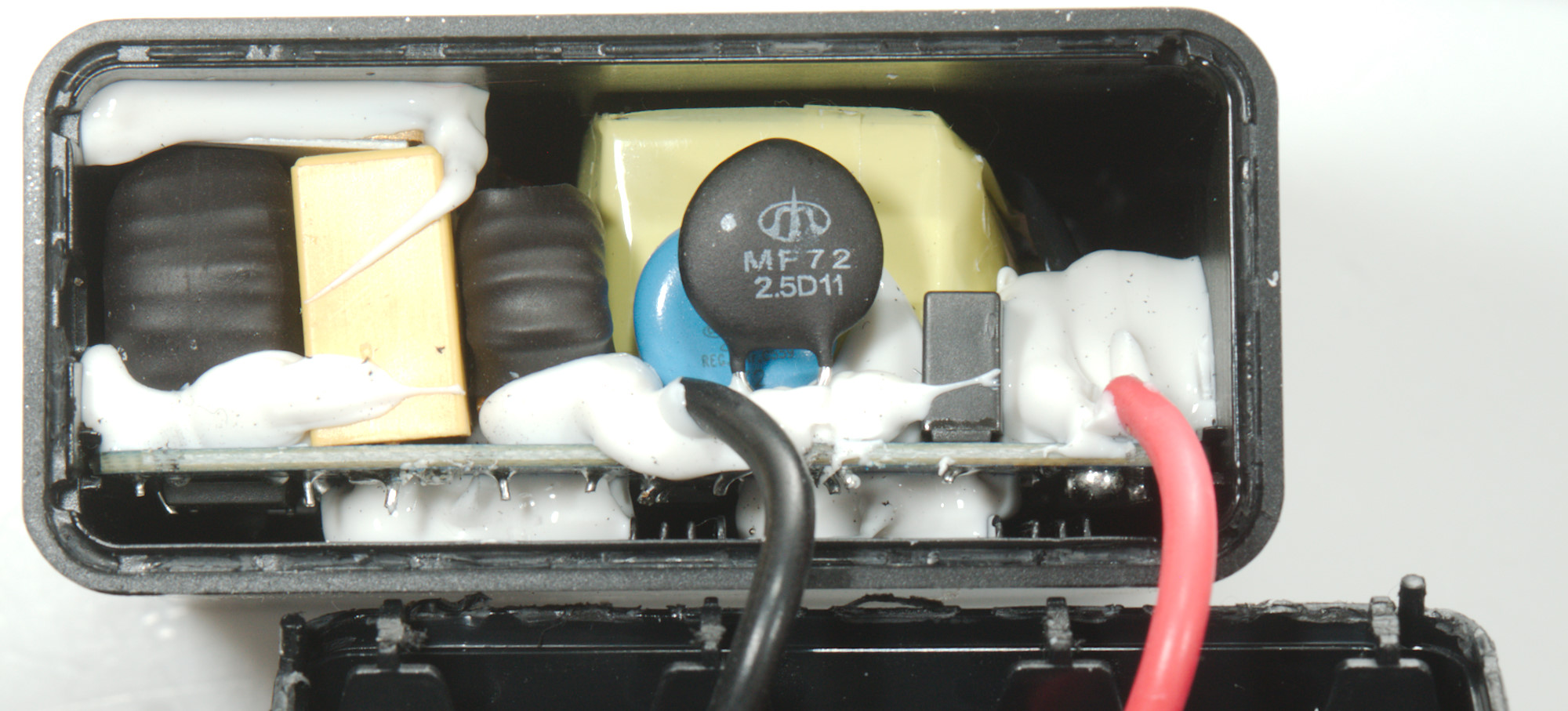
Mounting the bottom in my vice and whacking the top with my mallet I could open the charger, but getting the circuit board out is not easy, somebody used a lot of glue inside it.
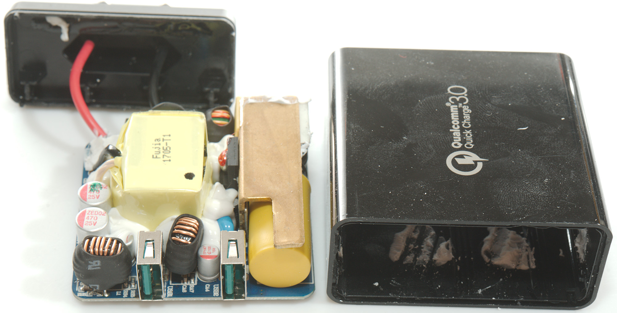
Loosing up the glue with a thin screwdriver and I could pull the circuit board out.
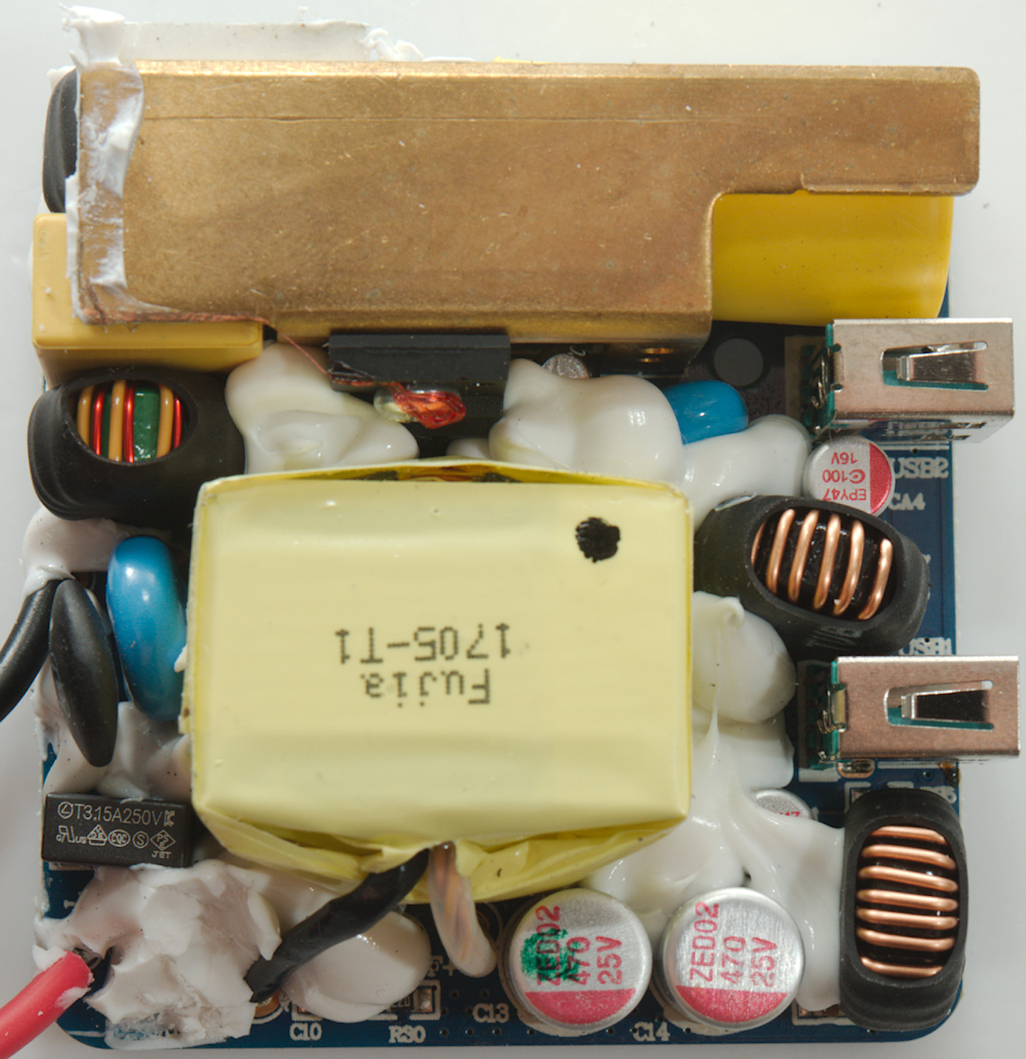
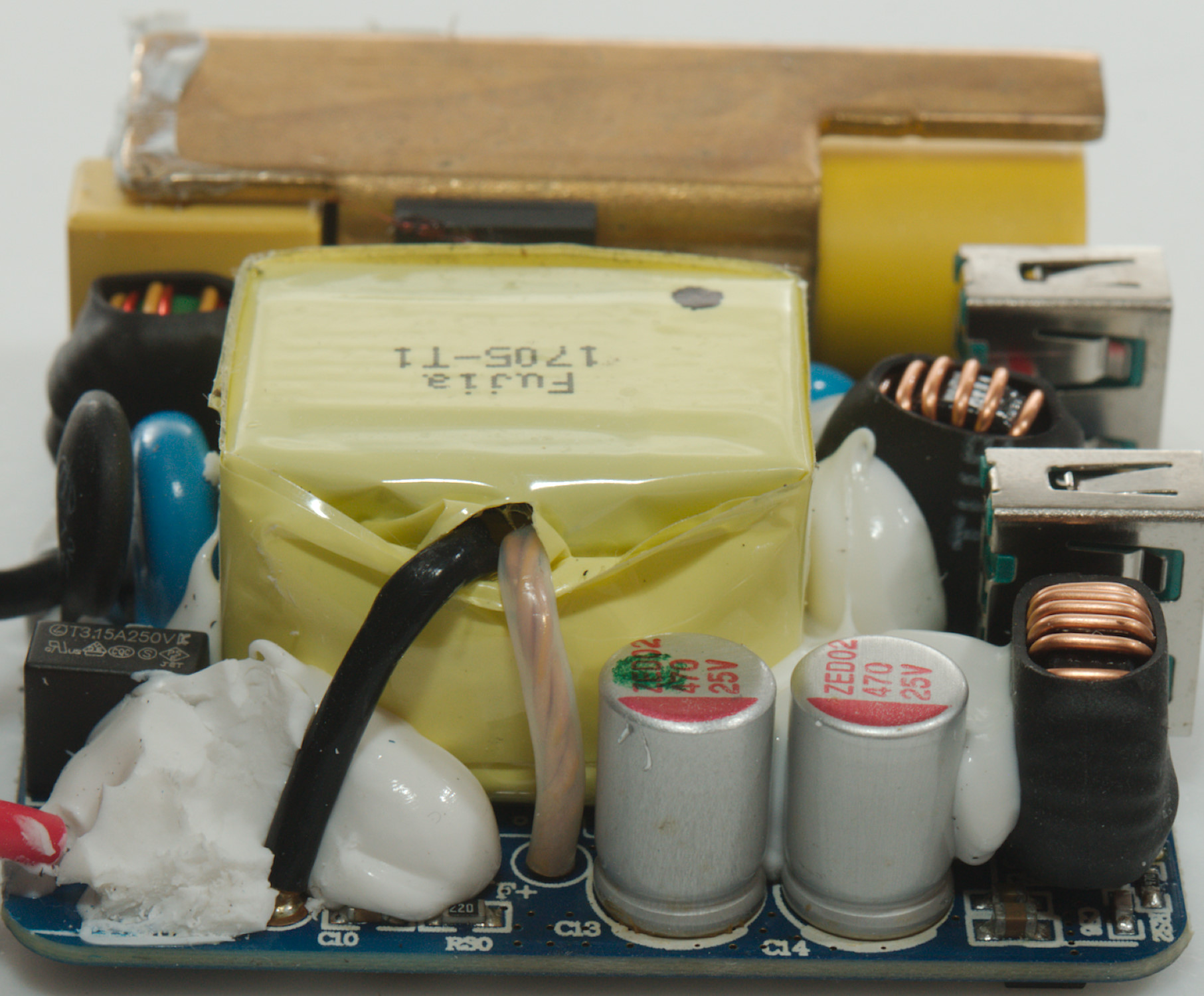
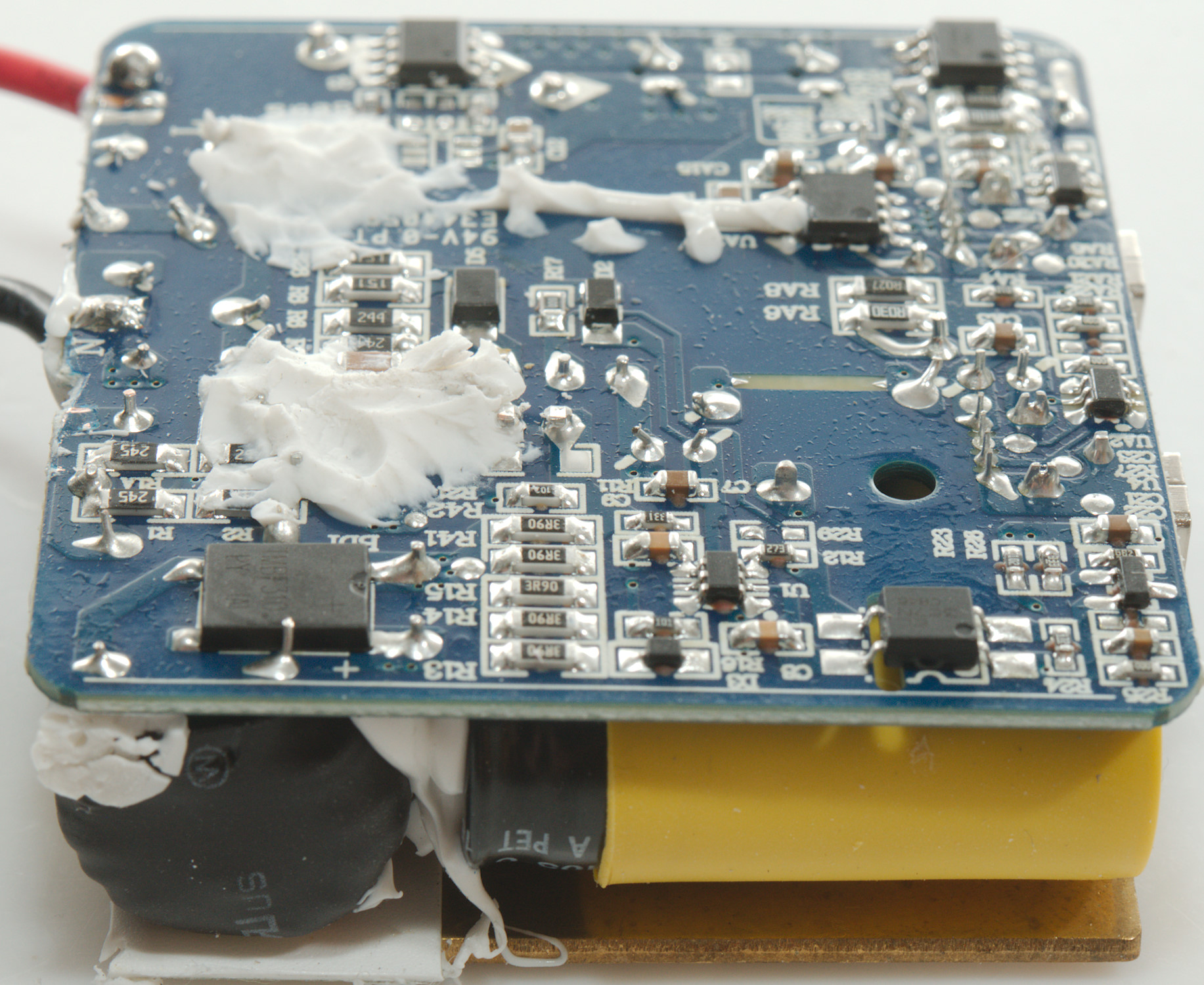
The circuit board is rather compact. At the input is a fuse and a inrush current limiter (PTC). There is two common mode coils, one is below the copper heatsink for the mains switcher transistor. The safety capacitor (CY1) can also be seen next to the heatsink. The mains smoothing capacitor is below the heatsink and has a yellow isolation cap on it because it is very close to one of the USB connectors.
The transformer deliver 14.6V DC output to the two smoothing capacitors (C13 & C14: 470uF 25V), this is then handled by two buck converters, each with a inductor and a capacitor (CA4 & ?: 100uF 16V).
Above C10 and RS0 is the synchronous rectifier controller IC.
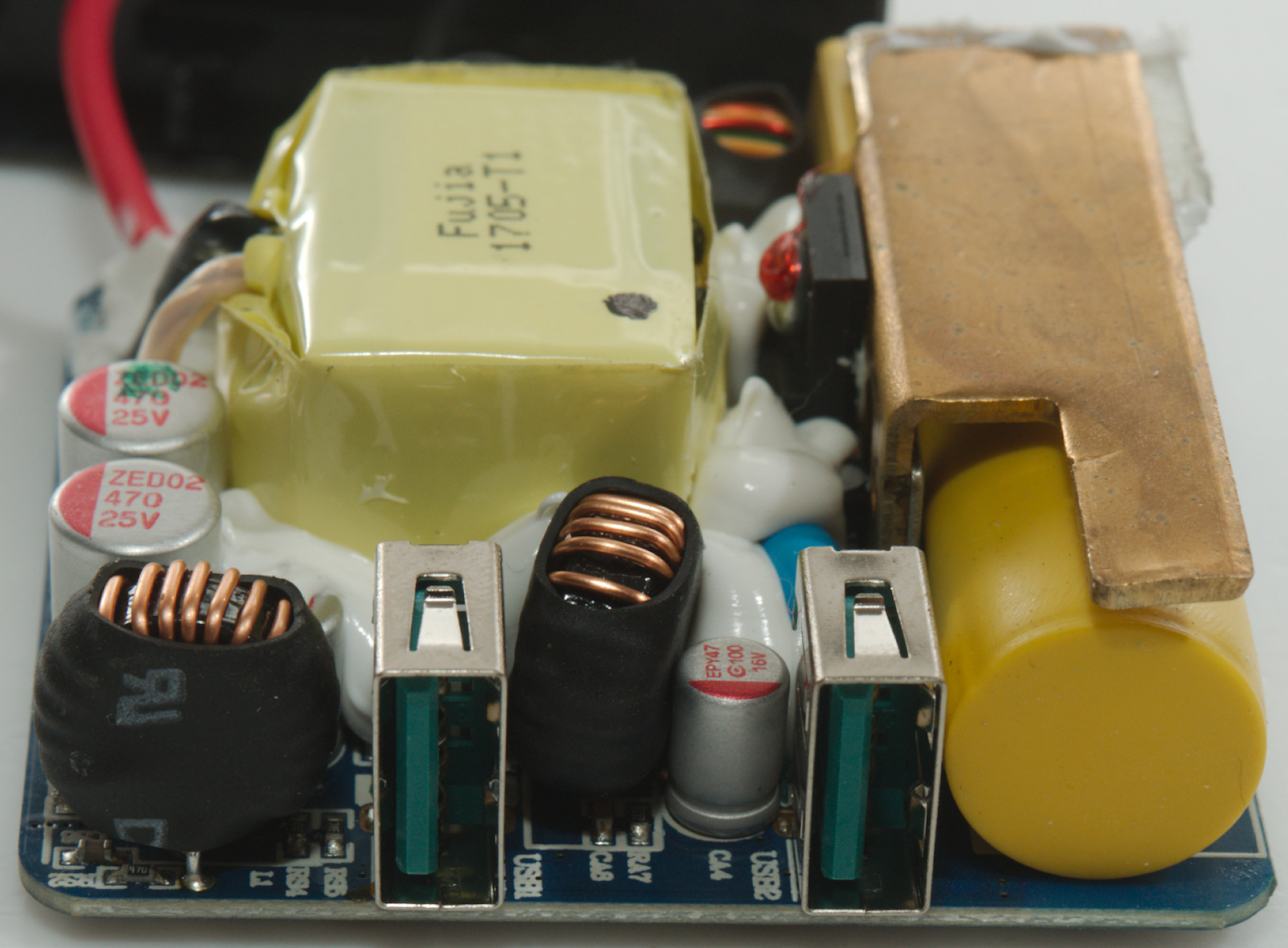
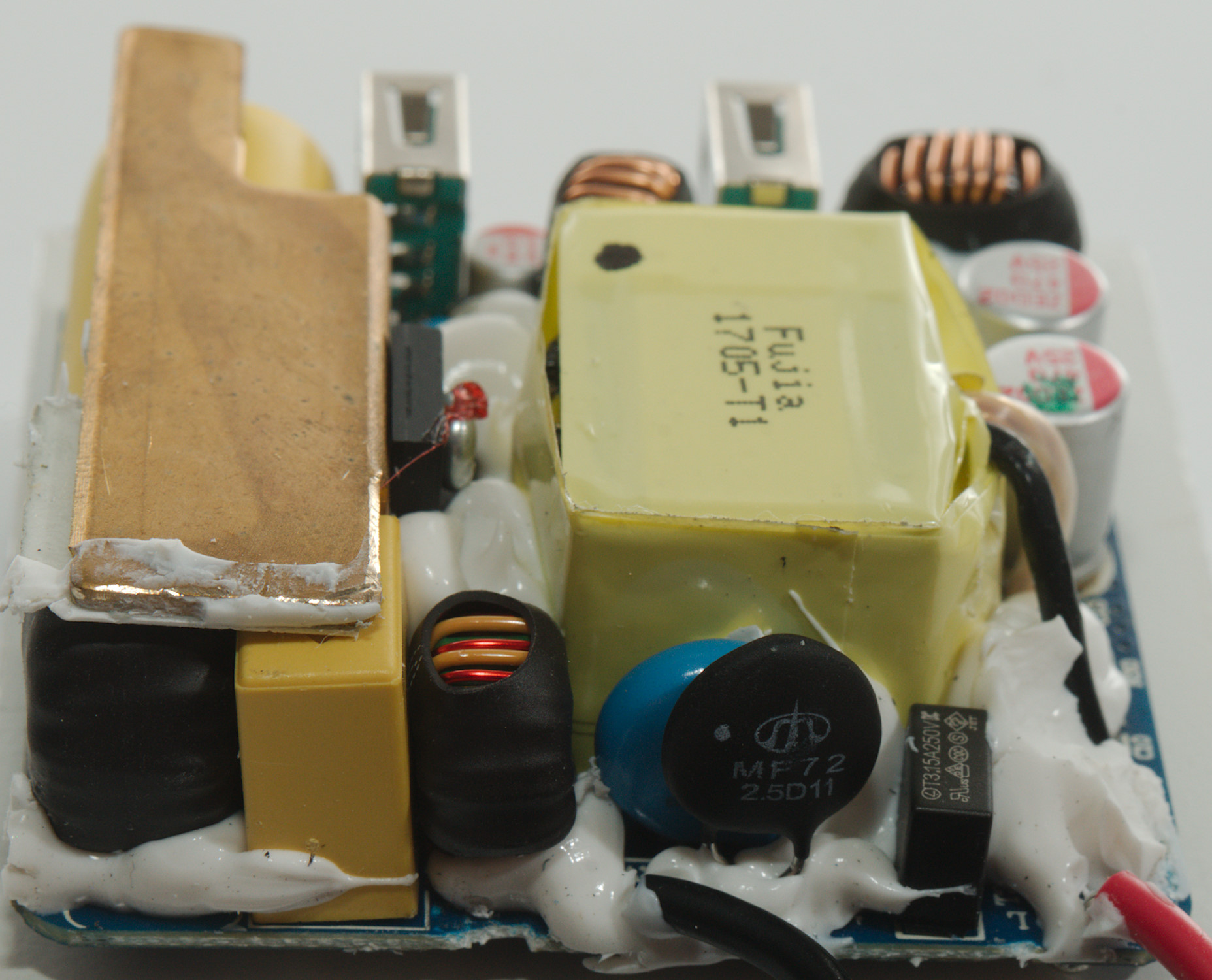

On this side is the input bridge rectifier (BD1), the mains switcher controller (U1: Marked OU=22C) very close to the opto feedback (U2) with the usual reference (U4: BM431). On the low volt side is a synchronous rectifier transistor (Q3: 10R12V). This voltage is then feed to two switcher (UA1 & US1: RH8605E) that reduced the voltage to USB level controlled by two QC controllers (UA2 & US2: Marked FT42JR)

Testing with 2830 volt and 4242 volt between mains and low volt side, did not show any safety problems.
Conclusion
This is a dual QC3 charger with enough power to drive both output fully with good overload protection. It do have a few codings to make it fairly universal and the output has very low noise.
I will rate this as a good USB/QC charger.
Notes
Index of all tested USB power supplies/chargers
Read more about how I test USB power supplies/charger
How does a usb charger work?