AVRISP Thinks MOSI is Shorted! Apparently it doesn’t like the RC circuit for the PWM. Knocked off the R1 resistor and C1 capacitor while I was at it and grounded the bottom side of R3. This makes it a pin toggle operation only at the moment.
Had too much paste on first reflow of the LTC3454 and came up with near shorts on pins to ground. Reflowed it, no shorts, but no go on powerup. Oops, had it in backwards, time for the backup chip .
Note to self, don’t allow ground pour to get between resistor pads next time
Now that I’ve got your attention; the 1.1A was only for about 30 sec when I pulled the power. Didn’t want to leave a permanent mark left on my temperature indicator (i.e. index finger ). Any longer on time, and the dreaded overtemp shutdown and blinky shortly appears. This driver chip is gonna need a block of ice. 1A continuous (per data sheet) my */@!
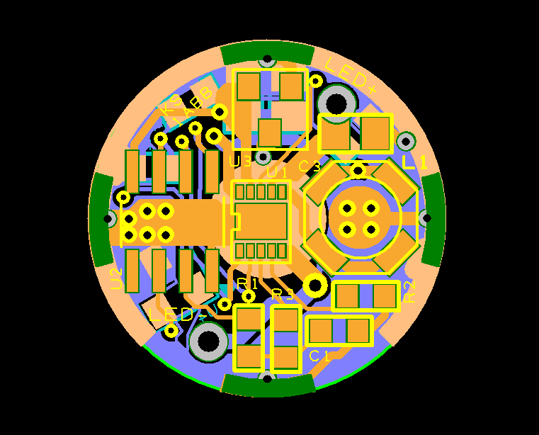
Part of the problem is my location of the LTC3454 over the battery positive area. So, thermal vias directly under the gnd/die pad not possible. Also a bigger bottom copper sink area is going to be required somehow. Potting the driver would probably also help.
Please note in rev1d there is a wider ground path on the top copper and some vias placed about 10mm away.
Still having problems with programming in circuit. Cut the MOSI trace and ran enable2 pin from PB3. Very sketchy, might need some ISP resistors. I would have thought the LTC3454 enable pins would have been high impedance. Another factor is that if both enable1 and enable2 lines are low, then the LTC3454 goes into shutdown, messing up the timing perhaps?
Hey Kent, I got my board the other day, thanks! Is the parts list the same as before? I have the resistors and caps you sent. I will order the rest on my next Digikey order.
Your welcome! Mostly same parts as of now, except the PWM location is set up for the 0C1B/PB4 pin of the ATTINY25V, in the skinny SOIC8 package (0.150” wide body).
Until a steady state HI setting is established, the Iset2 and Rset2 values will be in a state of flux. My original calculated values of Iset1/Rset1 of 250ma and 12.4k is very close to actual value. The Iset2/Rset2 calculation for 750ma and 4.12k ended up being a little high with around 780ma tested. My guess is a lower compromise value Rset2 will need to be arrived at due to the heat issues. Two or three intermediate values wouldn’t hurt if you are ordering. For instance a 6.19k is supposed to get 500ma:, So when added to the 250ma of ISET1, you get a 750ma Hi setting.
I started playing with Atmel Studio6, and gcc. Right now I’m using GCBasic. Code is just PWM’ing the Iset1 pin per the data sheet and turning on/off the Enable1/Enable2 pins with some delays in between. No battery or temp monitoring etc. yet.
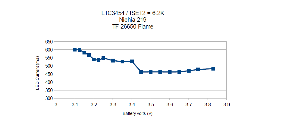
Here’s an interesting plot of the I vs V for the LTC3454. This is for a ISET2 resistor value of 6.2K (6.16K measured), and an approximate calculated I (led) of 500ma. You can see where it goes from Buck to Buck/Boost to Boost. It drops out of regulation in the blink of an eye around the 3.1V mark.
The previous post, and this one, pertain to my breadboard setup which has the LTC3454 on a smt to dip adapter that I made. The results could be better, or worse, with the 17mm pcb mounted in the pill.
I was going to make an extended run at 700ma (ISET2 = 4.22K), but I pulled it after just 5 minutes due to the heat issue. I’ve already smoked a couple of LTC3454’s from my thrashing about .
Off a fresh TF18650 Flame, and the 5 minute run at 700ma, there was a steady climb to 52.4C…….toasty! This was measured at a via in the ground plane very close to the chip.
If I take one more swing at the pcb board, I may try my first 4 layer fab. Having the two inside layers dedicated to the gnd plane could be the ticket for sinking the heat from the LTC3454 package? I’m kinda having a debate on this, because of the underwhelming results?
Only 52C? What is the TJmax of the chip? If it is 125C, then you should be good to 70 or 80C on the outside. Just a guess as I am going by typical junction to case thermal resistance.
I guess I’m the cautious type , thanks for the feedback. When the pcb goes in the pill then the ambient is going to go up, because of the heat from the LED. Check my figures?
125C max junction temp, 70C+ is in the guaranteed range, and 40C/W junction to ambient. The Rdson for the switching Fets are from the data sheet measured at 500ma, so the calculated Tj is going to be higher than below.
Assume roughly combined Rdson of say 0.34ohm and 700ma for current. Then P = (0.7 x O.7)A x 0.34 ohm, or 0.167W x 40C/W = 6.7C. Add that to ambient (52.4C) and you have 59C. There’s some headroom left, but good reason to have some temperature monitoring.
have you tested the board with it mounted to some kind of heatsink via the ground ring (ie. as it would be in a light)? Provided it stays within specs and there’s some kind of thermal monitoring and response via the Attiny25 thermistor, I don’t see a big problem.
It’s interesting how much variance around the set current value there is depending on battery voltage, especially in boost mode. Any idea what the current draw from the battery is at different voltages? Not especially important, but would be interesting from an efficiency standpoint.
The test rig has two 1/4” square pads connected by via’s. Once the pcb is mounted to the pill, then testing would be very difficult.
Can’t fully account for the LED current difference in the Boost mode. A significant difference can be attributed to the data sheets programmed current vs. Vin and Temp graphs of around 10%.
With a full battery (18650) 4.19V, ISET1 = 12.4K and ISET2 = 4.22K:
interesting and keep up the good work. It’ll be another couple of weeks (including a holiday, yay!) before I can put SMD to driver board so fingers crossed the wrinkles will all get ironed out.
odd about the PWM - do you think that might have anything to do with PWM frequency?
The buck/boost chip probably has a settle time requirement where it searches for the proper output level. Each time the PWM turns off the driver and turns it back on, it may have to go through this cycle. I wonder if this could be causing the erratic output results… maybe try lowering the PWM frequency which would lessen the percentage of time the chip is ‘searching’.
I know you have invested a lot of time/resources to get this project working with the LTC3454. Are you open to the thought of going into a slightly different direction? My main gripe with the LTC3454 is the Vin range of up to 5.5v, with a absolute max of 6v. This pretty much limits power sources to a single Li-ion. With a Texas Instruments TPS63000 (BPT) Vin is 5.5v, with a absolute max of 7v. This would open the door for use with 2 x CR123. I’ve been using Shiningbeam’s 3-mode perfect regulated circuit which uses the TI TPS63000 with both single li-ion and 2 x CR123 without any issues at all. This additional flexibility of power sources makes it a better choice IMO.
Edit: If you wanted more output you could go with a TPS63020 as well.
All possible theories. I’m running the PWM at 20kHz. The PWM goes thru a low pass filter (R = 100, C= 100nf) or around 16kHz. So there is some voltage attenuation on the PWM output.
Tried PWM at 10KHz and other than having to reset the duty cycle, I come up with the same PWM efficiency (70.1). Playing with the PWM duty cycle, there seems to be a linear relationship between the ISET1 current setpoint (236ma) efficiency (87.2), and the PWM setpoint (72ma) efficiency (71.2%).
I have sampled both those TI chips and have smt to dip adapters being made as we speak . The TI chips have come up before in PM’s. The TPS63000 chip has lower Rdson Fets involved, which is a good thing. Adjusting the TPS63000 circuit for constant current/PWM output seemed quite a bit more involved (more parts) then the LTC3454. So that is the reason why I decided to plow this road.
I learn by doing, so the exercise has opened up my eyes and helped me gain valuable insights on driver design.
Not familiar with CR123 batteries. Not sure how you square up the difference between low voltage cutoff of the Li-ion and the 2xCR123?
CR123 primary batteries have a voltage under load of roughly 2.5v @ 1A discharge rate. Please see details here at CPF for discharge graphs. On the shiningbeam driver I am using the low voltage protection is set to 2.8v. For a 2 x CR123 setup in series that would be 1.4v per cell. At this voltage point its not too low where there is a big risk of cell reverse charging.