I look at v2.0 since that fatter ground restricts placement to where you want them.
solderpaste is my friend:

Definitely not as slick as the other side, but still looking good:

wired up:

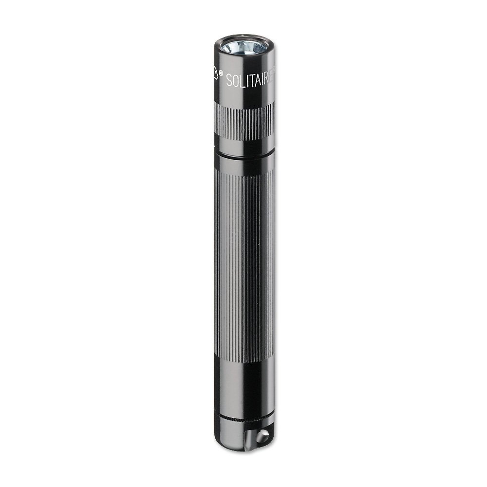
And it works, output looks like 350mA, all modes are there, no 'stars' were connected to ground, so since it was a standard 105C, it is low-med-high-strobe-SOS. So the bottomline is: reflowing makes life really easy. I will wait for V2, but I already love this driver, thanks Scott&Mattaus for doing this. (now, where is this driver going to go?? Too small for the Ultrafire M5. I may have to sacrifice my solitaire after all :-) )

SEE! THIS IS WHY IT PAYS TO REVIEW THINGS LATER ON, AND HAVE OTHERS LOOK AT YOUR WORK!
Sorry, I'm yelling in frustration. The reason I would have run that long trace from C1 to the GND pin of the MCU, rather than straight to the GND ring right freakin' beside it, is because when the schematic is drawn I connected C1 to P4. You can't really (Well you can, but it's impractical) account for the ground ring in the schematic. Eagle then places a an un-routed path between the two points. Unless you're really switched on you can easily, and blindly, follow what it's asking you to join up.
Kind of embarrassing really. I'll fix that up tonight and move that via out from under the pad.
TP, genuine question so I can further my electrical knowledge and PCB skills - why is a via under a pad a bad idea? The only problem I can see making it a bit more difficult for the component to "self locate" during re-flow soldering. But other than that? Maybe some weird resonance effects or something on the signal at the pin perhaps?
+1.
OSHPark is more lax when it comes to routing. I used to use Seeed more and their routing is a bit more accurate. Regardless I will make the GND ring larger so that it should be right to the edge regardless of who makes the PCBs.
Also, in regards to Helios' requested regarding D1. If I shift U2 up and left I can probbaly fit D1 beside it, leaving more room in front U2 for all your stacking needs.
I'll make TexasPyro's and Helios' suggested changes tonight and post V2.2 up for review.
We'll get there eventually!
- Matt
All my rambling has been merged into the post above.
![]()
Looks like you and I were tandem typing Matt. Please ignore that raving Texan regarding shifting Led- but + on the rest. Maybe a 7mm centerd circle in a layer somewhere as a guide to fit the pieces into? U2 doesn’t need to be centered but it and D1 both have to fit. Also, Can the ground via at upper left be enlarged to wire size like Led±?
I’ve been enjoying working with everyone on this. It’s been a fun project and will be great to be able to use the results of all this time and effort. Yours in particular, Matt.
Nice job Djozz! You’ll have to show it off. How many will you stack?
Oh no, peer pressure! I am very bad with that...

Yeah, I hate the way Eagle handles traces like ground rings that are not drawn via the “route” command. It basically does not know they conduct electricity and make for a valid circuit. I usually wind up routing a trace under the ground ring made up of lots of little line segments… or just ignore the air-wires (risky).
Having the via in the middle of a surface mount pad can cause problems soldering the board. It reduces the pad area available for solder to flow, etc. If the component lead winds up over the hole, it may not even make contact. Maybe not an issue with a hand-soldered one-off board.
OK, thanks texaspyro. I'll be moving it all tonight. I do the same with Eagle; in fact I don't even run a design rule check anymore because I find most of the time Eagle has no idea what it's talking about. In the end I almost just free draw my PCBs and ignore any whinging Eagle does!
What an amazing effort from an extraordinarily clever bunch of guys. My shout fellas. ![]() Well done.
Well done.
Gorgeous!!! Better than some "stock" jobs right outta China
What temp did you have your hot plate at...def going to do the reflow...I'm afraid I would solder like "Mongo" on these tiny components!
Ordering 2, unless you guys know where I can find em cheaper
Yeah...a direct 10440 in a XR-E would be VERY nice! (once you visualize it...liiightbulb)


Very cool explanation, much appreciated.
V2.2:

Some notes:
1) It's not possible to move the VIA under the 6th MCU pin. I know it looks like it, but in Eagle there is just not enough space without being precariously close to something important.
2) Ditto for moving D1 to beside U2. I did move U2 up and left a bit because it was sitting over the LED+ VIA previously. Now there is nothing covering the hole at all.
3) I increased the size of the ground pad on both sides so it now sticks over the milling line completely (light blue circle). What this now means it when it's milled, it won't matter if the fabricator mills from the inside, middle, or outside edge of the milling line; it wall always have copper right to the edge of the board.
As always please review and let me know what you think.
- Matt
Gorgeous!!! Better than some "stock" jobs right outta China
What temp did you have your hot plate at...def going to do the reflow...I'm afraid I would solder like "Mongo" on these tiny components!
I guess the hotplate is a bit above 200 degC, but I never measured the temperature. For led reflows I set the power supply at 10.7 V and let the block temperature settle for half an hour. Under 9V solder will not melt. even not direct on the block, so I guess the block is not too far above solder melt temperature (180degC). I did this reflow at 11.0 V.
POW, cheaper
off topic but I just had to say: I hate amazon ![]()
looks great Matt, but couldn’t that via in question move slightly back towards the MCU, maybe .5mm or so, such that it’s out from under the MCU leg and on the other side of the board the trace from the chip catches the side of the via instead of being right on it? Looks like it could move over almost the diameter of the via and be tucked behind the MCU leg and still feeding the chip just fine. My 2 cents.
Like this:

… and while you’re at it could you make white solder mask with pink silkscreen…. JK ![]()
c’mon people, are we really going to shuffle vias and traces .5mm back and forth, does it work = yes, good, now mass produce it :bigsmile:
I like oshpark’s purple the best. Maybe light green or orange silkscreen if it was free (or even available!) ![]()
When working on a 10mm board 0.5mm can make a difference.