Pics of your build please ![]()
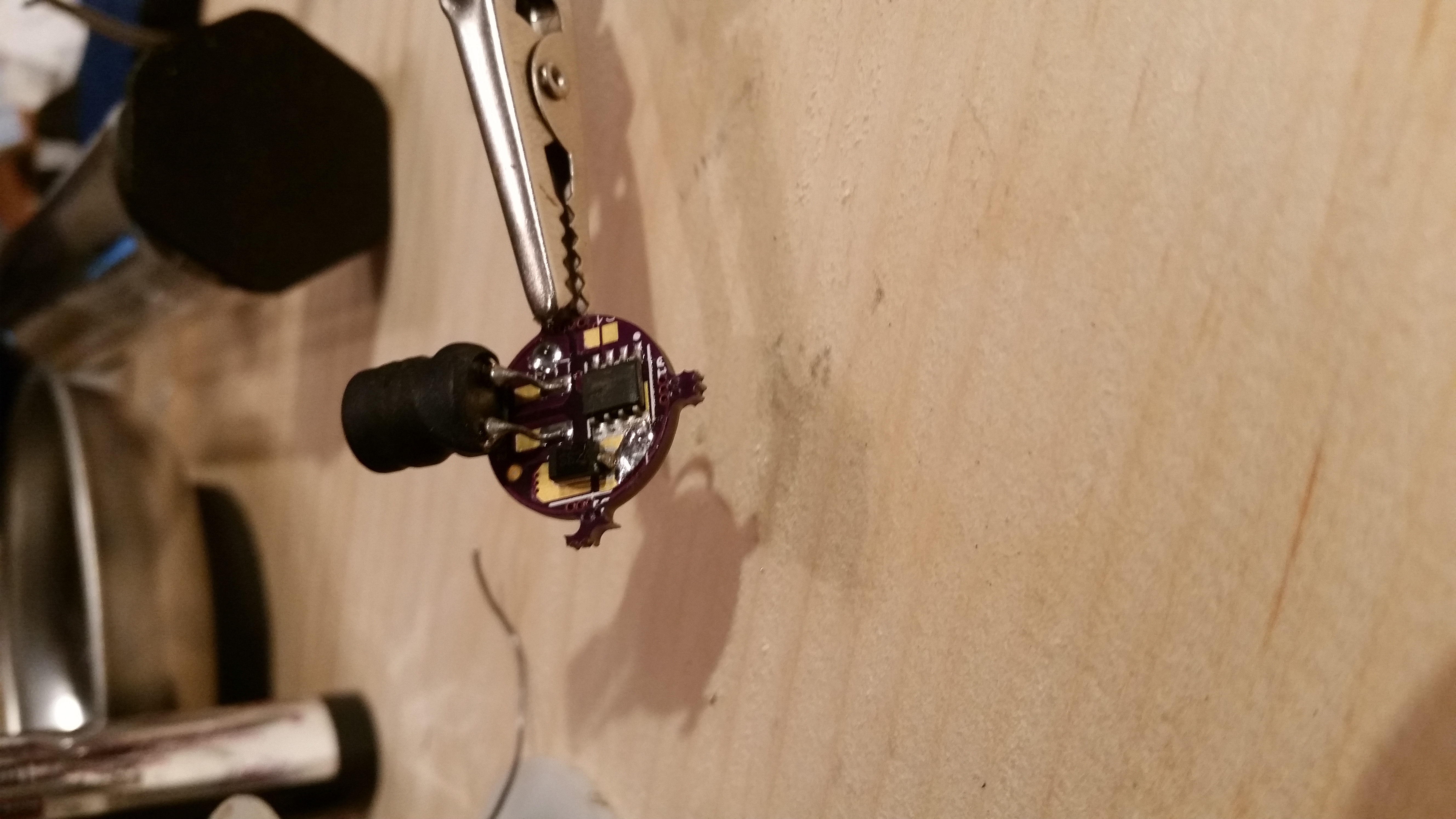
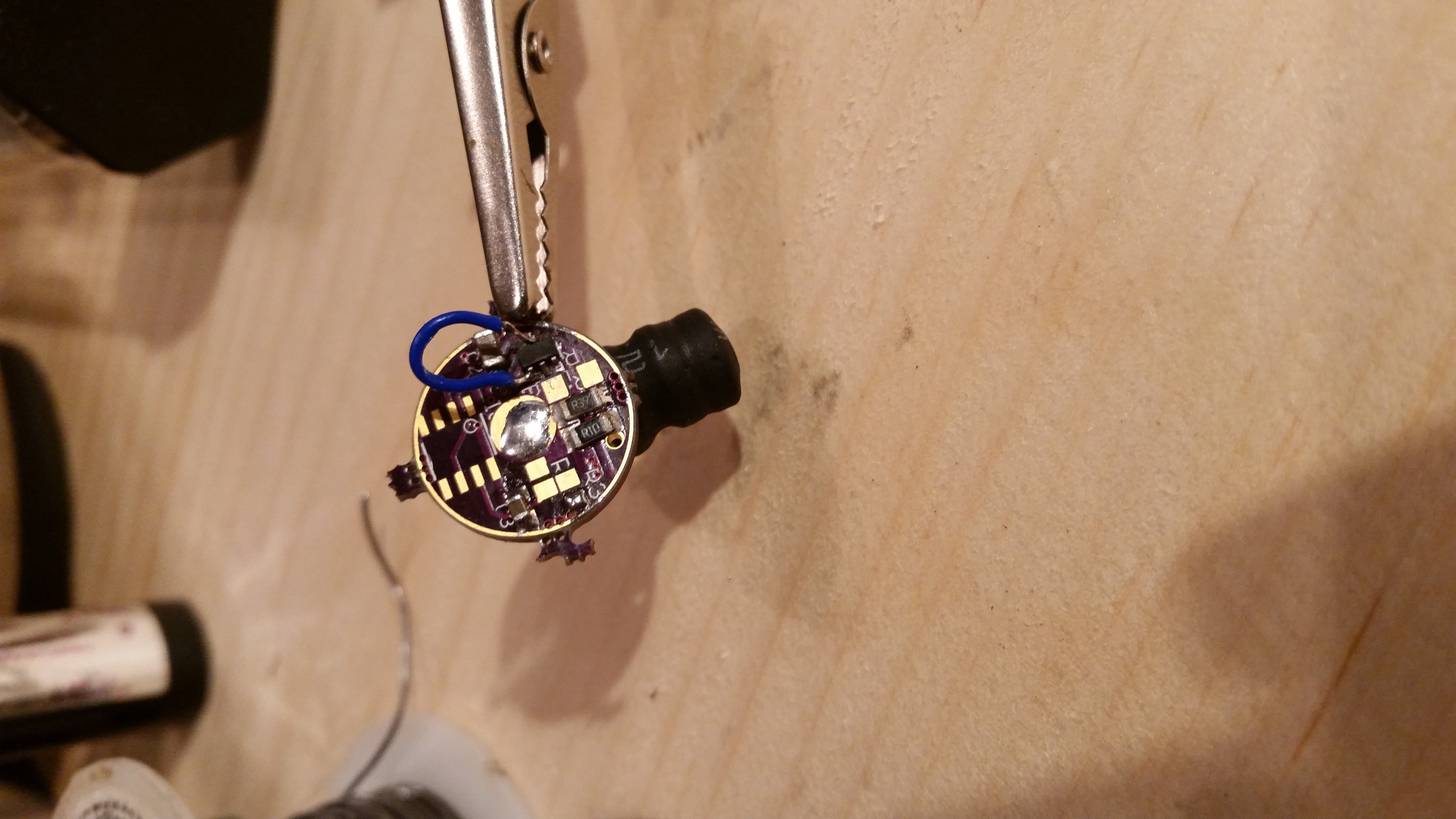
Phone pics may not have been the way to go, these are pretty bleh:
Nice…love the purple board goodness!
More bad news. I moved the components back to the stock PCB and they function in that configuration. This appears to be a layout issue.
EDIT:
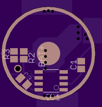
I’ve reviewed the layout again (of course I looked closely yesterday as well!). (See post #41 for the layout) I do not see any problems. Sense trace is short & thick, gate trace is about the same as the DX board. LDO cap is a long ways away but shouldn’t matter? Input smoothing cap is very close.
So I’m going to put the components back on my PCB again. ![]()
Good luck, fingers crossed
Still no luck. I got the same results as the first time I populated my PCB - low current at low voltages, higher current at higher voltages.
I tried:
- removing the cap on LDO (greatly reduced current)
- input voltage = 5v & strapping the DIM pin to that instead of to LDO (no real change over using LDO)
- moving my GND point next to the FET (no change)
- leaving DIM floating again (no output this time. this pin is not meant to float, so this means nothing.)
Tonight I did some bone-headed experiments which really proved little to nothing. I killed both of the QX5241 chips which I was willing to sacrifice for now. I ripped the leg off of one and miswired the other.
I’ve ordered some more chips.
Wouldn’t it be nice if a flashaholic worked for one of the chip manufacturers and could sponsor our research. A few chips invested here and there to promote the sale of many more.
Much as I love free stuff, I’d rather get free advice!
Plastics…
As in invest in?
I think so. The Graduate ‘One Word: Plastics’
I preferred Harold & Maud.
I don’t think I’ve seen either, but “invest in plastics” was such a thing, it must have permeated lots of creative works.
Looks like I could move the QX5421 to the top if I also move the input smoothing cap and sense resistors to the top and move the diode to the bottom. If I did that I could make the DRV (gate) trace much shorter. I don’t see the length as the issue though. There must be some no-no that I’m unwittingly committing.
Sorry wight but I’m helplessly hoping here.
Bad news first: I still don’t have anymore QX5241 chips. The eBay vendor sent me AOZ1014AI instead. Hopefully I can get them to send me the right thing.
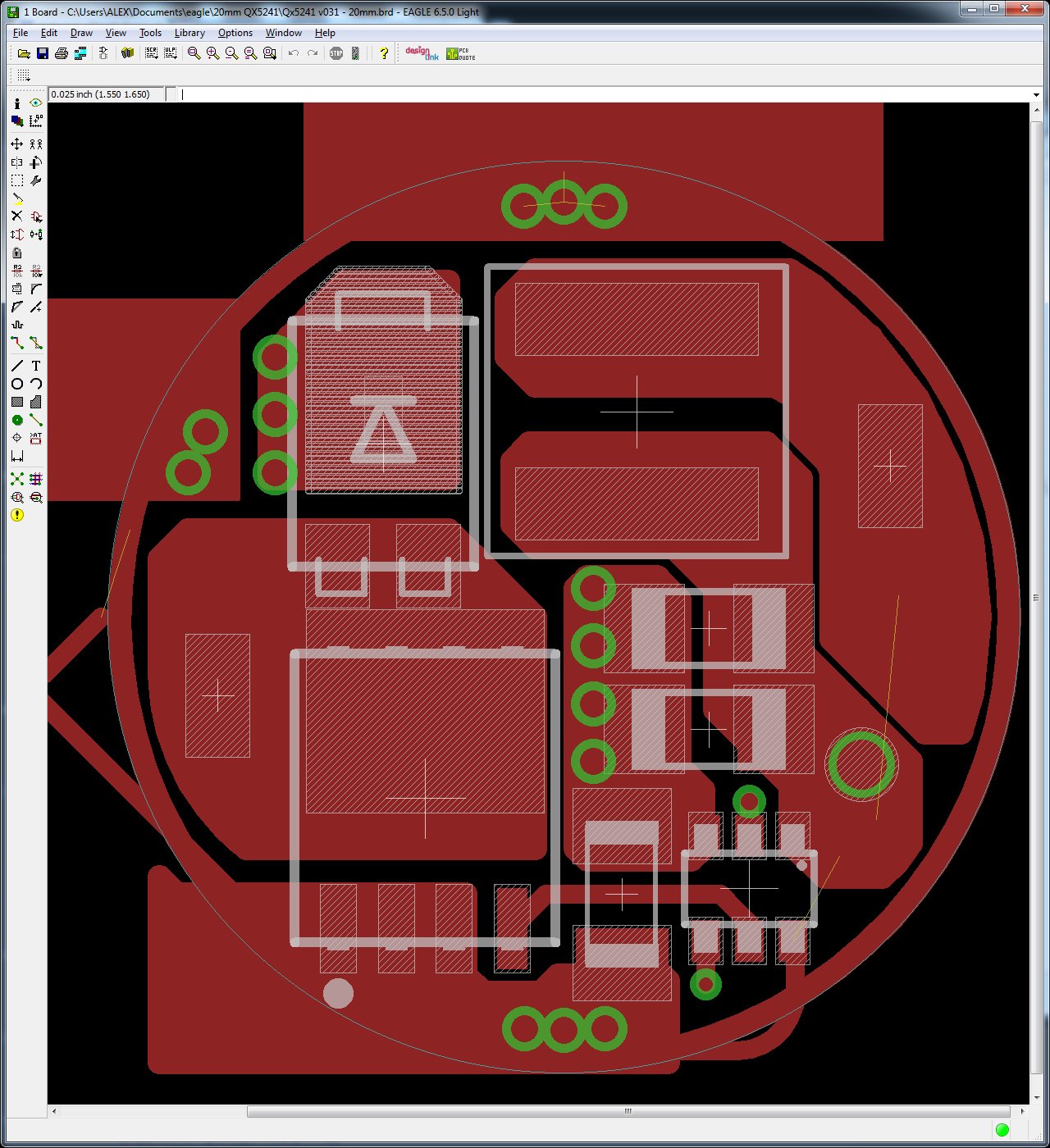
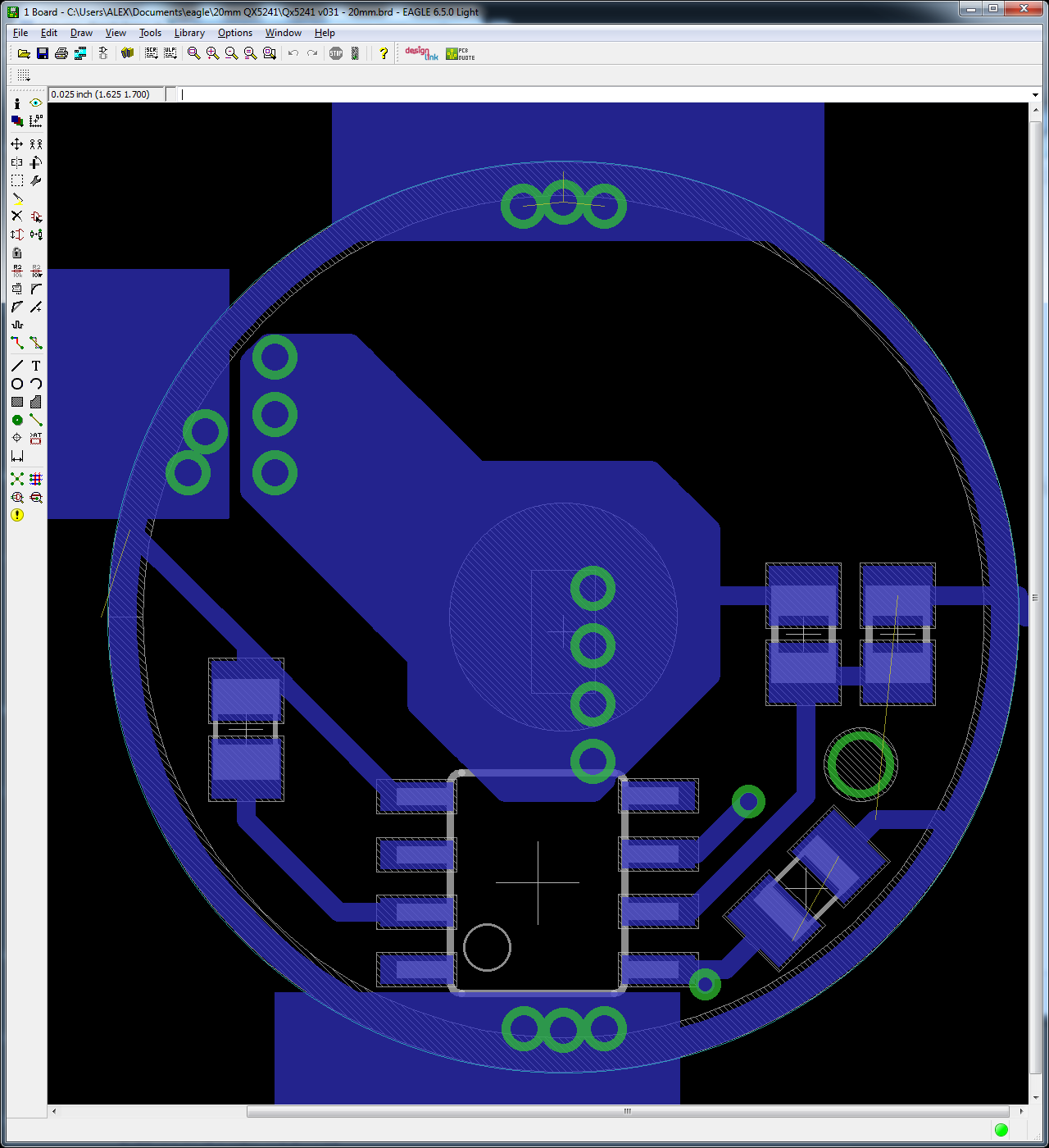
Good news now: I haven’t given up hope, so in preparation for eventually receiving some more QX5241 I’ve decided on my next troubleshooting step: a new PCB layout. I wanted to put the entire buck section on one side, so I stepped the size up to 20mm for now. Even with the extra 30-40% more surface area this was more of a challenge than I’d hoped. Therefore I sacrificed a sense resistor - the design is now down to two of them, at least for this 20mm test version.
I’d like to say that I did a ton of improvements, but I still don’t see any problems with the 17mm version. As far as I can tell my decoupling cap placement is great on that board. Maybe it’s the location of the Vcc trace. That’s my best hunch. Maybe when I get some more QX5241 I will cut the VCC traces on one of my existing 17mm boards and relocate the Vcc cap for testing.
Any way you cut it, this one is now super simple! I know the layout is a train wreck aesthetically. Despite my continued hope and effort, I’m nowhere near motivated to clean this up until I can get something to FUNCTION.
Please review. No aesthetic suggestions, only functional considerations, errors, etc please.

Good news #1: the seller did indeed deliver my 5241a chips on their second try! I’ve had them for several days.
Good news #2:
- I received the 20mm boards today.
- I built a 20mm board with a single R400 and it regulated fine at 0.5A output to an original-gangsta XM-L.
- I added an R39 in parallel to the R400 and the driver regulated fine at 1.0A output to the same XM-L.
I tried putting an R10 in parallel to the R400 but it seemed to go DD. The R10 was used so maybe it was fried from being soldered so many times. I will continue to work on this.
I have now tested with:
- (R100) = ~1.8A regulated.
- (R100 & R39) = 2.2A regulated.
R100 & R39 is the stock configuration of the donor board, DX SKU: 20330. As far as I’m concerned, the buck section of the 20mm board has completed phase 1 testing. I have not installed an MCU & support hardware.
What is the max amps you can push? I would really like one and drop into a Defiant super thrower and push it at around 3-4A w/ 2 18650’s or 26650’s
Most awesome man!