Not burned off as heat. Do you know how a FET works? You can have a different voltage on 1 side than you do on the other, it is not burned off as heat though.
Don’t know about Field effect transistors. I thought 7135’s are constant current sinks that turn excess voltage into heat. The reference to transistors was comparing the Vdd pin to the “gate” of a transistor. Just looking at similarity to what it does as opposed to what it is. For perspective only.
The bolded statement is correct. 7135 chips DEFINITELY run hot pushing low Vf emitters with 4.2Vin. They generate enough heat to be “painfully” hot to the touch after ~.5-1 second of gentile touch pressure…. IMHO hot enough to require additional cooling methods.
Thanks for the useful thread - this should be a sticky, IMO.
Agreed. The data sheets seem to indicate the possibility of handling up to 4V excess(see dropout voltage vs output current graph) which translates to ~ 1.5W PER CHIP. Also indicated is the heat sink area at various thermal resistances. Up to 1000mm^2 of copper trace area to sink each chip. WAY more than is present on a 17mm board. I have often wondered how much better the chips would do if they were not backed up against another high heat source like the LEDs. I have always tried to separate the led and the driver as much as possible even though it adds some extra wire.
I recently did that on a build. The 7135 drivers were so hot I could not keep my finger placed against them for more than a second without pulling away from the pain. The 10x7315 chips got very hot MUCH quicker than the XML running at 3.8A. I added cooling fans and pieces of 22AWG solid opper wire to try and sink and radiate heat away form the double stacked chips.
I have always wanted to try making my own driver “board” by using 10x chips, 20-22AWG solid copper wire and stringing the drivers in a row parallel wired.


Better question - Do You know how a FET works? You can’t simply have a different voltage on two sides of anything without it acting like a resistor (Ohms law Applies) and a FET is really just a variable resistor when being used as a current limiting device (AMC7135). If you draw 350mA through a FET and one side of said FET is at 4V while the other is at 3V, then I promise, 1V * 350mA = 350mW is being dropped and converted directly to heat. In that situation, the FET is being gated to act as a 2.85 Ohm Resistor.
Even the datasheets of a FET will explain this. At different gate drive voltages the RDS (Resistance from Drain to Source) changes. This is how the AMC7135 functions - the control logic varies the FET gate voltage in order to maintain a RDS value that allows 350mA (or 380mA) of current to flow.
PPtk
I do know how a FET works, but it’s been a few years since I’ve looked at them much, but you are right. I think I was actually thinkin more of a BJT anyway and in an amplifier situation i.e. an audio amplifier where you aren’t controlling to a constant current etc.
Amen, sticky!
If you can link your previous thread including Ma_Sha’s CPF link you have the beginnings
of one helluva sticky sir!
Kramer5150 - If you PM me your address i’ll send you some special wire or “wet noodle”…Amazing stuff
Thank you for clearing that up. I did not understand the original fet reference but it seemed contrary to what I thought I knew which is this:
Any supply voltage above the Vf of the led is converted to heat.
Above 700mW additional heat sinking is needed to keep the junction temperature below 120C.
The 17mm boards have nowhere near the copper trace area needed to provide the additional heat sinking needed.
The output current vs dropout voltage(excess voltage converted to heat in the chip) curve cuts off at~<4V.
4V x 350mA = 1.5W
Applying 2.7-6.0V to the Vdd pin causes the chip to turn on allowing 350-380mA current to ground.
I do not know what kind of cryogenic cooling was used in their testing to get that performance but the wattage is of the same order as an led and should receive similar treatment.
If any of this is in error. I would like to correct it now so please, chime in.
Anything like this?
Here is the first prototype showing led- out(white wire), two ground wires left and right that slip into the ground vias of the mcu board, and a Vdd wire (small bare wire) to connect to the mcu
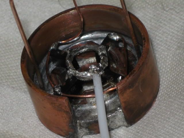
That proto worked fine until I cooked the chips trying to reflow more copper onboard.
Here is a pic of the next prototype that will get the chips added late tomorrow night
More cu gets added to direct the heat through the housing to ambient.
If you’re curious you can follow this. I appologize if it’s a tedious read but the thread contains some usefull bits and is ongoing.
Wow thats intense.
But yeah I think were on the same page. I got a bunch of these HS from work and my thinking was to just line up the 7135 chips in 2-3 rows. Thermal paste them onto each HS and just string solid copper wire across each in parallel.

One thing I noticed while I had my light apart was that the 7135 chips were CONSIDERABLY cooler running when I ran my light on the two lower output modes. Its only the 100% EPROM program where the heat build up became alarming.
This surprised me, knowing that the 7135 converts excess Vin to heat. Vin is still ~4.2V, Vout is still ~3.2V… where does the heat go?
One more question… do higher ma BIN’d 7135 chips run hotter than the lower BINs?
I have been using the 380 mah BIN’d chips from illumination supply.
thanks!!
The reason is that heat is watts, and watts are current * voltage.
assuming (rightly so) that the Vf of the emitter doesn’t change all that much (negligible) from the low current setting to the high current setting, the math is as follows…
Low Mode (lets say 350mA @ 3V)
1.2V * .35A = 420mW of heat
Med Mode (lets say 1A @ 3.1V)
1.1V * 1A = 1.1Watts of heat
High Mode (Lets say 3A @ 3.2V)
1V * 3A = 3Watts of heat
Remember that the heat is from the voltage drop times the current through the chips so the lower modes having less average current generate less heat. Each “on” pulse generates the full amount of heat but the lower duty cycles have more “off” time with no heat generated.
I hope that makes sense and that I have it right
Yes, the higher binned chips should run slightly hotter due to the higher current.
You have it correct.
The definitive thread on slaves is ” the sought after master/slave sandwich mod-an explanation” started by Justin here but there are a few things I wanted to add.
Any amc 7135 board with an mcu can be used as a master(not just 8x 7135 boards) and if the led- pads on each board are kept separate then each board could have a different number of chips supplying a different current to each led.
What would be the easiest way to connect two of these boards in order to obtain a single led driver that pushes 2* rated current of each single board to the led?
And am I correct in assuming that you can disable the Attiny controller on the second board by simply cutting the leg from the Attiny going to the trace that is common with the Vdd trace of the 7135 chips?
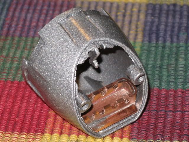
On the picture that is the third leg from the left in the upper row of legs. That is opposite of the "dot" the chip has for orientation.
TY for any help :-)
That is a master/slave mod where both outputs go to the same led. You are correct about the Vdd trace/mcu pin but some boards use a different processor so I identify the Vdd trace as being the one that connects all of the right-hand pins on the 7135’s.
Easiest would be to cut or desolder the Vdd pin on the mcu.
Connect the two boards together Vdd-Vdd, Output-Output, and ground-ground. I solder the Vdd and Output jumpers onto the first board, then use solid wire posts in the ground vias to hold the boards together and then connect the jumpers to the upper board.
I first heard of this over at C*F done by Stephan but I’m sure it’s been done here as well if anyone would care to donate a link to this thread.
Stacking chips is another option that uses less space as you do not need an extra board or wires.
Edit- On certain boards( like the 105C) you can connect multiple boards using solid wire in the vias (small holes). I use VSM (very small wire) taken from stranded copper power cords for the Vdd link and SSM (sorta small wire) drip system wire for the output and ground links. The soldermask has to be scraped from the surface of the trace around the vias on each board. The output vias are too small for the wire guage needed and need to be reamed. Care must be taken to preserve the trace and solder the link to both sides of the board.