I was thinking two channel, but really it makes no difference. Just run Pin3 instead of Pin6 to the 7135’s on the bottom of the picture.
Yeah, I think that’s where my problem is though. Pin 3 is on the other side of the MCU from pins 5 and 6. I think if I squeeze my LEDs in toward the center like your drawing, giving more clearance on the ends, all the traces can get to where they need to go. It’s all the criss-cross stuff that is holding me back. I’m going to work on it some more tonight, if I can get the chance.
Remember you can run traces under the mcu and between other pins. You definitely need to have traces outside of the last emitters as I have drawn, but you don’t need that much clearance. Just remove the vias on the outside of the emitters and you’re fine.
Just orient the MCU with Pins 5678 to the right, in my head I think that should work fine… right?
Thanks! I didn’t get to work on this at all last evening. I was having computer mouse trouble. Actually, the mouse quit working while I was trying to work on the driver. Then, I finally got one to work, but my wife needed the computer. Then, by the time she was done with it, I had given up on doing any driver design, and had found something else to do. So I never got back to it. Maybe tonight.
Maybe some ideas from this bad sketch(pleading bad hand)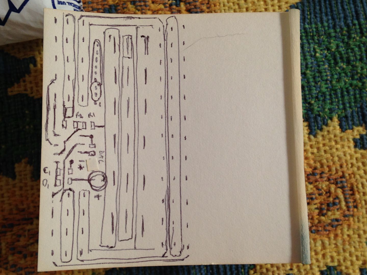 I suggest you don’t use autoroute as it cannot intuit your ideas. Note the use of components as trace jumpers.
Another thing, you want to leave as much copper on the board as possible. Think of the board as a solid copper surface that you are separating into different signals.
I’m starting to think there’s a bit of misunderstanding about the board size. You guys are drawing pictures that are a lot taller than the board I’m trying to make. My constraints are 16.5mm x 64.5mm, roughly the size of a 16650 cell. I know the picture in the OP doesn’t look like that, so maybe that’s where the confusion is coming from. It’s a lot of stuff to pack into such a small space.
I worked on the board a little more last night. I still haven’t figured out how to get all the signal traces to where they need to go without crossing each other. If I’m not going to use the bottom for traces, then NONE of the traces can cross each other at all. They each need a dedicated amount of space on the top of the board to get to where they’re going. I’m using all but a couple of the pins on the Tiny13 chip, since my design is for three channels. I also have six LED pads on the same board with the driver components. These things combined make it extremely complex and challenging for me, being the newbie that I am. I still haven’t given up, but I’m getting frustrated.
Edit: I also haven’t yet tried out all the suggestions given so far. So, it’s far from over. Just venting here. ![]()
How big of a physical keepout do you need around the emitters for the optics/reflectors?
Mattaus wasn’t a newbie and it took a few months to hammer out the design of the tiny 10. Don’t sweat it. There’s no scale on my drawing and no reason it can’t be made the size you want, specifically the LEDs and their traces and can also be made narrower and folding R1/R2 and moving the OTC. I mainly just did it to show how to route signal traces under components which auto route won’t do. What you want to do is possible, it’s just a matter of trying different ideas and seeing which works best. Just a suggestion but most of the difficulty is working around the mcu, the LEDs and 7135’s are mostly rubber stamped so start with the mcu and auxiliary parts layout and don’t bother with the rest until you have that sorted to your liking. I agree that daisy chaining the 7135’s is the way to go as it allows the LEDs and 7135’s to share the same trace width on the - side. You can adjust the size of the annular rings on vias to be able to cram more of them together without overlap and the ones in the center pads need to be untented to fill with solder.
I don’t need physical keepout at all for reflectors on this light. One big lens/cover will be over the top of the whole board. But, OSH Park gives you three copies of your board. So, I’m designing also for the future possible use of boards two and three. I’d want to keep at least 3-5 mm away from the flat sides of the LEDs, I’m guessing. Someone who’s done lots of modding would know better.
Thanks, RBD!
You can’t cross traces but you can use components to jumper across and there are more than enough to accomplish this. Physical separation needed is less than you might think and signal traces can be a lot thinner than power traces. Even mcu power can be narrow. Plan the layout to use these notions. Look at some of the existing designs to see just how thin, narrow, and tight things can be. Push the 7135’s right to the edge of the board and the signal trace will still be safely inside. The width of a 7135 is 4.6mm(max) so that leaves 7.3 mm for the LEDs, + trace, and a bit of separation on the minus side, plenty. ![]() Nine 7135’s on the mcu side will take ~47 mm(need set back from the ends for signal trace and clearance) but that still leaves 18.5 mm of board length down that side and bending the led+ trace (center pad trace need not be continuous) between the middle two LEDs will give you more room. The mcu will probably need to rotate 90 from my sketch so I’ll see if I can run up that part of the layout but the rest should be no problem.
Nine 7135’s on the mcu side will take ~47 mm(need set back from the ends for signal trace and clearance) but that still leaves 18.5 mm of board length down that side and bending the led+ trace (center pad trace need not be continuous) between the middle two LEDs will give you more room. The mcu will probably need to rotate 90 from my sketch so I’ll see if I can run up that part of the layout but the rest should be no problem.
RBD, the MCU is dipping down well into the space between the LED pads. Add the C2 under that, and there isn’t any room left for a LED+ trace to cross from the left side to the right. Other than that, I’ve got your sketchy layout working on my board now.
Edit: Wait a minute. I have the MCU sitting lower than it needs to be. Be right back…
Here’s another set, this time to scale although I can’t draw .1524 mm trace width or spacing. 
 I suggest 1.8 mm 7135 GND and led- trace width.
Well, this is what it looks like from your first sketch, RBD.
![]()
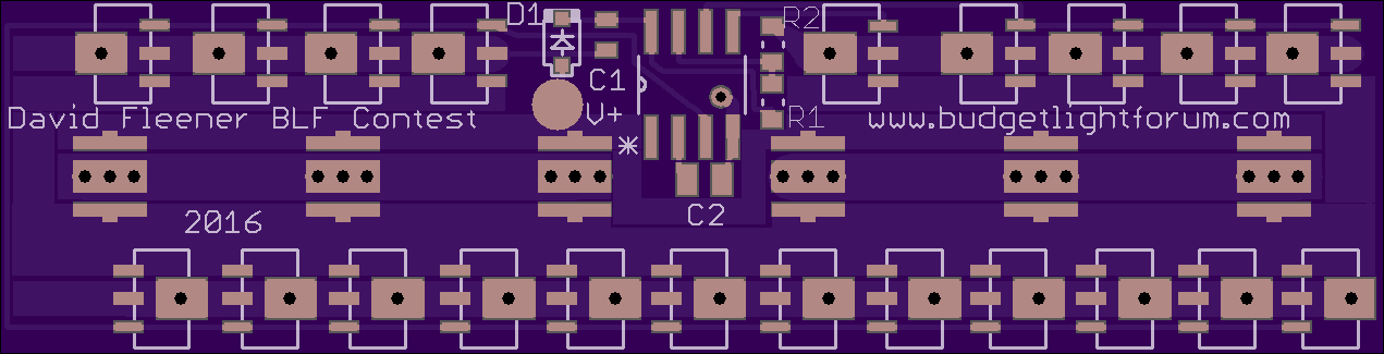
So, other than making it look prettier, do you see anything I need to change? Have I done anything wrong on this one? I think the only LED trace that is less than 1.8mm is the LED, because space is tight. I guess I could drop the LEDs down from center of the board, and make the LED trace wider that way. Would that be worth doing? As you can see, the top half is crowded, but the bottom half is more spacious.
Are your caps the size in relation to each other that you want? Normally the OTC is the smaller one. Also keep in mind you won’t be able to get your clip on the mcu with the cap that close.
LED+ looks really really close to some other traces as well, but that could just be the render.
Where’s B- or where you just going to solder to a ground tab? I’d spread out the 7135’s along the length unless there’s an overwhelming reason to be a masochist. Shifting them will open up more real estate for the mcu and it’s parts as well allowing more options for placement/rotations, etc. I rotated the mcu because it’s shorter that way and placed all of the auxiliary components off to either side with room to solder and eliminates the dogleg in the B+ trace. C2 looks tight and easy to bridge to the wrong pin. Trace clearance is one thing, soldering the stupid things is another. Led- looks severed at the right end of the board, could be just the render though. Your version looks like it would work but some changes will make it easier to build.
-Edit, fill that center pad trace with vias, untented ones will allow for more solder, heck, a bare trace would allow you to solder a 12g wire on board. Also, increasing the size of the bleed areas next to the LEDs will make them easier to solder by hand unless you plan to reflow them.
Yeah, I don’t know about any of that stuff. That’s why I’m asking for help from you guys! ![]()
I really appreciate all the help you guys have given me, and any more that may be offered. I never intended to invent a new driver board for this contest light. I would say it just kinda happened, but really - fritz made me do it! :smiling_imp:
So, do I need to switch the caps? I was trying to follow the Mattaus tutorial when I started. I thought I connected everything in the schematic the same way he said. But, I could have screwed it up.
I forgot about clips on chips, too, with this board. I was just trying to get the components to fit. I’ll move some stuff around to get more clearance. I don’t program MCU’s, but who knows what I’ll be up to with one of these boards in the future? I might as well make it as good as it can get in every respect, so I don’t have to redesign it yet again some day.
The traces are very close all over. I blame RBD for that. He said stuff could be crammed tight, so I believed him. ![]()
My Batt- is going to come through the back of the board. That’s why I made it a ground plane - there’s no paint of any kind back there! I hope OSH Park doesn’t complain. :money_mouth_face:
When I do my tidy up, I’ll move all those 7135’s into a perfect cadence, evenly spaced across the board. I crammed them over to the right side in case I needed space on the left side for traces.
I did cram the C2 right up tight to the bottom of the MCU. I was trying to get as much trace width on LED+ as possible. I’ll probably drop the LED pads down a little to relieve space in the top half, and move that cap further from the pins, to lessen the chance of shorting.
LED- does look severed on the right side, now that I look closely. I used rectangles, and I thought I overlapped them but maybe I should check it and make sure when I do the tidy up board.
6mil minimum trace width/separation is only .1524 mm or damn close together. I’m more concerned with solder pad separation when the signals are different and copper is exposed. Under solder mask it’s more a fab issue as long as you obey the minimums and round off the inside/outside corners.