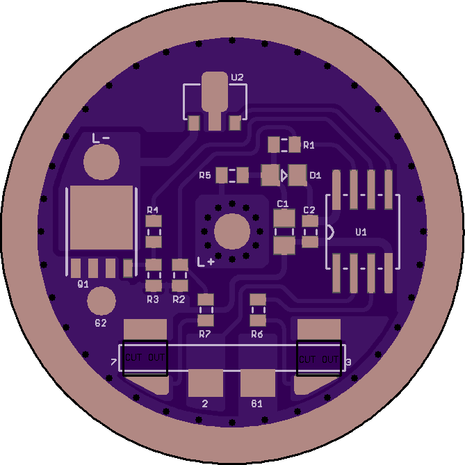
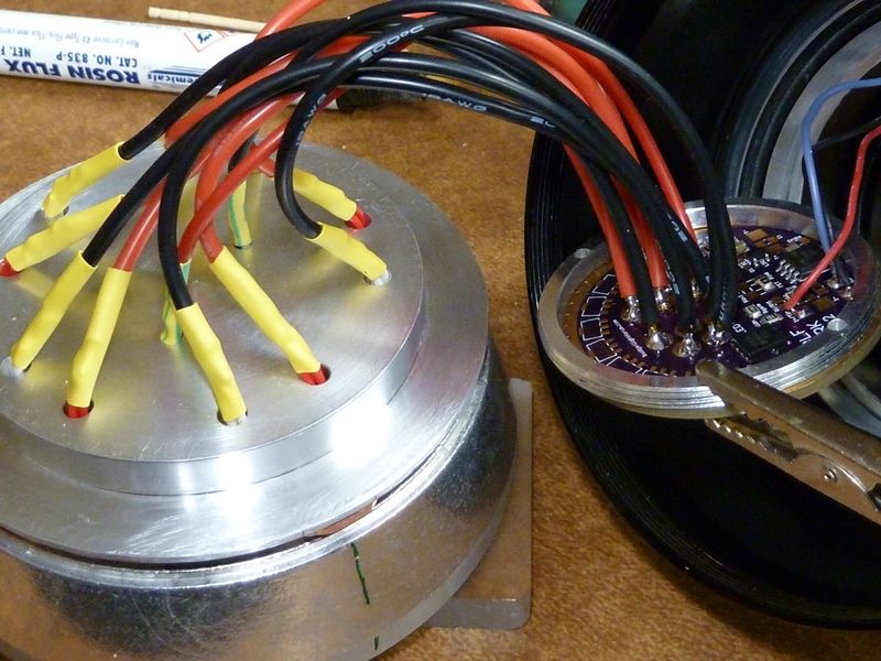
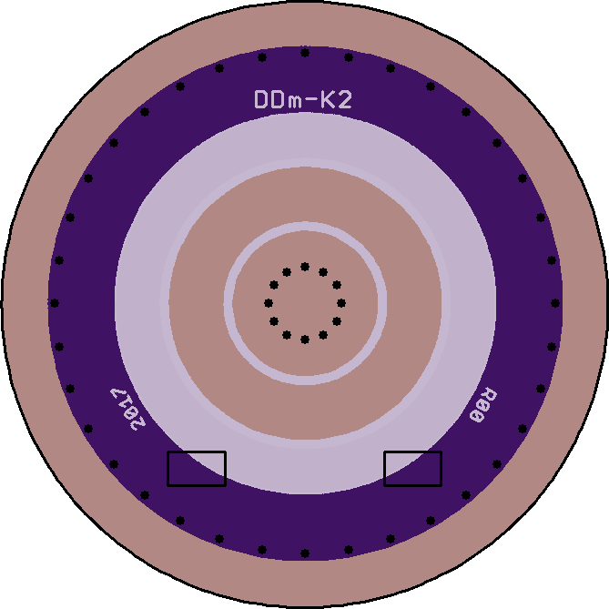
Synchronicity. I started on boards for the Fandyfire/Solarstorm K2 light. And now there is a sudden resurrection of these lights in several threads .
The K2 board is 34 mm in diameter and therefor relatively expensive at OSH-Park (compared to the usual 17/20 mm drivers). But for some reason I like these lights want to have a neater solution than the current piggybacks I am using.
Still a WIP:
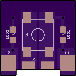
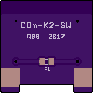
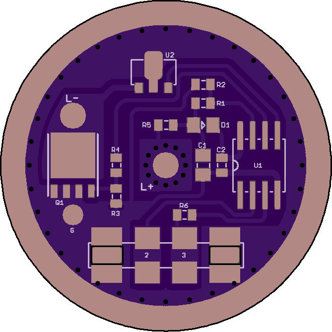
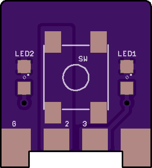
It goes together with a new switch daughter board, although I will try to keep compatibility with the stock switch board. The button is a 6.2x6.2x3.1 mm SMD tactile, similar to the stock button. LEDs are 0805.
The two indicator LEDs are in parallel at the moment. I could add some resistor/jumper options to apply MCU pin 7 to the second LED, if someone has use for it.
Another improvement would be to add pads for another one or two 7135s, allowing the builder to pick the regulated current level.
Dang, yet another practical board I need a few of... . The K2 is built like a tank for the housing, just the re-movable press-fit pill is not so good. Love the size/form factor, SS bezel, switch LED's, 26650 stocky light so a good tail-stander. Better than the SupFire L5 for sure, though I really like the Lumintop SD26 now, but price can't compare.
It's back to $20 at GB now, but still a good deal at that price.
Is there a reason why you don’t include a hole for the positive cable?
I really like it because you can solder the cable directly to the tip of the spring, route it through the driver and solder it directly to the positive pad of the led.
On your driver for the Yezl I drilled through the board to route the cable, so space shouldn’t be an issue.
Tom, any opinion on what to do with that second indicator LED?
For the K2 I agree the press-fit pill is not great…and also the glue-only option to hold the driver board in place …and then that big spring in the tail…but, like you, I still like it for some reason.
It is just a preference. For me it is a neater option and I can re-solder the emitter wire as often as I want without touching the spring. I did measure the voltage drop over those vias on the Y3 driver. 2 mV at 5 A IIRC, so the technical gain would be very little. I also use phosphor-bronze springs, rather than wire bypasses. They are not near the performance of a bypass, but they are ‘safe’ (do not self-heat at high current) and provide a little bit of current limit (I know…blasphemy!).
In the case of the K2, there is of course no driver-side spring. On the stock board I did have to add a solder blob on the center pad to get reliable battery+ contact. That is the purpose of the smaller central +pad on the OSH board as well.
Could to do dual versions in the future. One issue would be placement of the through-hole. It should be inside the base of the spring. So center of board would be ideal. This could be tricky on some boards.
For me I'm doing them in parallel on other lights, using as the single indicator LED. The problem once again is lack of I/O pins. In this case I could do voltage monitoring with the 1.1V ref, and have pin#6 to use for a 2nd LED though. Then sure, could use a RED led for low voltage indicating, periodic blinking it, etc. when the main LED is on.
Still did not finish that K2 board set. Internal cut-out dimensioning seems to be severely limited at OSH and I will probably change to simple surface-mount for the switch board. Not as durable, but with large solder pads it should be good enough.
The two indicator LEDs are now driven from separate MCU pins, with an option to drive in them parallel. Populating R2 / R7 and/or R1 on the switch board controls the options.
What do you mean by “Internal cut-out dimensioning seems to be severely limited at OSH”? What is it that you’re trying to do? Have you looked at the Internal Cutouts and Slots page?
On the K2 driver there is a little daughter board that holds the tactile switch and two indicator LEDs.
This daughter board slots into the main driver board at one end and into the emitter shelf on the other end. So it is pretty robust against button abuse. If you look at my driver board above there are two small square cutouts shown (labeled ‘cut out’ as recommended on that OSH cutouts and slots page). The two tabs on the daughter board would slide into these cutouts before being soldered in place. These slots need to be square and not much wider than 65 mils. But, if I understand well, OSH officially only support cutouts done with a 100 mils router bit (unofficially down to 40 mils). So best case the slots will not be square, worst case the slots will not be made at all.
Tore down my K2 mod last night - noticed one of my grnd wires to the piggyback driver came off. I was using a "cerial_killer" 17 mm board at the time and it had a very thin top grnd ring, so it didn't solder well there.
Debating whether to upgrade to one of your 17's now or wait for the new K2 driver. I got two more K2's to mod, so would definitely do these 2 with the your K2 board.
DEL (or anyone) - question on the single 7135. I used an LDO based FET+1 (SIR404DP and 350 mA 7135) driver for driving a whole bunch of XHP50's. After just a couple mins of use, of random ON/OFF, max power, ramping, etc., it appears the 7135 died - light would no longer shut off on the e-switch, but output about the level of what the 7135 does at max. Ramping of the FET still worked fine, as did max output. Granted there are actually 16 XHP50's driven from a 2S3P 18650 setup using fully charged Sam 30Q's, so tons of amps/watts are goin on.
What do you think? Should I replace the 7135 and try my best at heat sinking it, or dump the 7135 altogether and use one channel (FET) firmware?
Look'n at the specs, the 7135 is only rated to 6V or 7V, but it's been stated before here on BLF it should work with an 8.4V power source.
Okay, I just looked at it again. I see what you mean. What about using drill hits? OSH Park doesn’t support overlapping drill hits (they say the fabricator would just delete them) but you could still do a “perforated” outline using drill hits placed close together, which you’d have to punch out yourself. Drill hits can be very small, and you could even do vias for the added benefit of the holes being copper plated through.
I should get the K2 board out by the weekend. But it is going to be more than $10 for three boards and then there is the cutouts issue.
Do you know for sure that it ran hot? It should thermally limit itself and there are two other (more likely) suspects:
Brand of 7135. Some are apparently lower spec. than others.
Inductive kickback coming from the drain on the FET during FET PWM. I can imagine that this is impressive with the current and amount of wiring in that light.
I would try a known good type of 7135, run it at 100% with the FET off for a while. See if it even gets hot and/or throttles. Then repeat at 0% with the FET at 25% PWM. Then repeat at 100% with the FET still at 25% PWM. Try to see which of the three conditions kill it.
No clue now what killed it, if it was hot or not. Might have to rig up something on the bench then. hhmmm. Definite got some issues to accomplish this. Still don't have a working laptop, and have no computer near to my bench to do firmware upgrades. It's a big risk moving this open setup around. Gotta work out something though. Here's what it looks like:
It's HQ's triple channel SRK board, but configured for std ports, two channels. For the single 7135, he does have the full pad on the PCB for the pad under the 7135, so maximizes the ground/heat sync.
Ok though, I'll see what I can do for doing those tests. The 7135's I'm pretty sure all came from FastTech, though I got mixed batch purchases over time, but the marking are all the same. I could try a part from a different strip though.
Looking at the SRK rev3.2 board on OSH, the lone 7135 does have a full-size thermal pad, but not much more.
That pad is supposed to be part of a copper surface significantly larger than the 7135 itself. In our use a good thermal connection to the ground ring would help a lot as well.
I deliberately used thermals as a compromise. I saw more risk in killing the 7135 with excessive heat while reflow-soldering (killed a FET that way…) so I decided against full copper connection but used 3 thermals.
This could of course be manually fixed with braiding after reflowing, at least for testing purposes.
To the 7135 and 2S (8.4V). RMM long since warns against using them with 2S while comfychair always argued it would be ok.
Reading the datasheet I believe 8.4V exceeds specs. I tested it on my 11+1 x 7135 dual channel driver (2S, MT-G2) and let it run for 9 days in a row on the single 7135. 350mA no PWM at day, 35mA PWM at night. Changed cells often to keep voltage as high as possible.
Not only did the single 7135 survive, it has no reduced mA or visible output difference.
This is no scientific approach, I just wanted to know if I can kill the 7135, which I couldn’t.
So far, so good.
But: This 11+1 7135 driver has indeed 1.8mm copper connection to the GND ring, while the 3 thermals add up only to 1.2mm. So TomE, I’m very curious what you will find out.
Hhhmmmm. Yea, might do a quick&dirty try with a 2nd one. I looked carefully at the OSHPark design, and what HQ has is the middle pin unconnected, a full pad under the grnd of the 7135 though, then 3 small traces coming off the tab end connected to the ground plane. I'm sure there were routing issues, but the connection to the grnd plane does look a little light there. So I could do something there to help, like scraping off nearby covered grnd tracing to the tab and solder blob it all together, or solder on a solid wire from the tab to a nearby scraped off grnd contact. The outer ring is about 100% covered by the retaining ring, so I'm hesitant to solder anything onto it.
Wondering if a copper or alum heat sink thermal epoxied to the top of the 7135 would help.
I'd still like to do what DEL is recommending though to isolate it down, but might be better with something easier to bench test.
Ahh, HQ. Didn't see your post when I wrote above. The amps in this light is certainly insane, so there's been nothing like this done before, as far as I know. Vinh's 40K Fenix RC40 mod has no posted details, so we have no clue what driver, etc. He also has a 100K lumens AceBeam X65 mod in progress. In this one, only thing he posted was one picture showing some massive heat sync on some SMD part. Rumors are Richard built a 30K+ monster from the TrustFire TR-J20, but no details on it as well.
So far I love that mine is a 30K+ UltraFire, a true Budget Monster , not some $500 light used as a host, plus a relatively compact size.
Interesting test HQ. I also doubt that heat is the culprit. For reflowing, I guess the trick when DIY reflowing parts with big thermal pads is to pre-heat properly. I am usually more concerned for small parts twisting or tomb-stoning when there is no thermal relief on one pad.
Re. the 8.4 V, the chip should not really see that. Pin 3 is driven from the MCU. We have an LDO? So maximum 5 V here? Pin 1 is in series with the main emitter. So maximum around around 4.4 V here when only the 7135 is working.
When the FET PWMs it creates some impressive spikes on the FET/LED junction. This is due to the parasitic inductance of the LED wiring. This is also worse at higher FET currents. Pin 1 of the 7135 ties in here. With this light the wiring and currents are ‘worse’ than usual, so I would expect some impressive spiking. This would be my main concern. Not sure if the 7135 would handle it better being on or off when the FET is PWMend.
Two workarounds would be an RC/RCD snubber around the FET or a honking free-wheel diode around the LEDs. The main switching diode on a buck or boost driver should be suitable for free-wheeling if you want to borrow one somewhere. I have also seen some older Chinese FET drivers that include this diode.
max spec on the 7135 is 700 mW with up to 1000^2 mm trace area per chip so I don’t think it’s simply a voltage issue. Less trace area and more shared heat seems likely to limit that. Most drivers have very little trace area and lots of emitter heat and can handle only about half that. I think it’s a real good idea to use a generous (and continuously soldered)ground pad as del did with a large ground pour.

 . The K2 is built like a tank for the housing, just the re-movable press-fit pill is not so good. Love the size/form factor, SS bezel, switch LED's, 26650 stocky light so a good tail-stander. Better than the SupFire L5 for sure, though I really like the Lumintop SD26 now, but price can't compare.