Thanks Halo... and Mike C. Yes, OSH Park since this will probably just be on minimum quantity order of 3. I'll download their rules. I used the Net command. Maybe that includes the Signal function.
Can drills overlap?
Doing so flags a DRC error, but I don’t know if OSH Park care or not though. I’d ask them (or other intended fabricator) if I really needed to know.
No, oshpark does not allow overlapping drills. Drill hits can overlap the board edge but not other drill hits.
Its mentioned on the “Verify your design” page, where you review the preview renders of your board:
All the xpe library parts were generated so they don’t work on the default grid and net command can’t connect. Aargh! The XML part works fine but ain’t the right one.
Thanks to Matt’s videos, I was able to figure this out enough to get 99% there. Now my problem is Oshpark not rendering what I want it to render. Drills appear non-existent, and for some reason the top looks like it’s not recognizing the board dimensions. Any thoughts?
Here is my:
Osh Link
BRD File
Gerber Zip
I remember seeing this tiny board issue but don’t know what it is. Are you doing drills or vias? They’re not the same. Vias link traces of the same signal on both sides of the board -use “name” command to make them the same. Are the various layers in the right place in the gerber files?
I used vias but I didn’t name them. Does it make a difference?
I’m still pretty hopeless with eagle. It takes hours and there’s always something wrong so you should probably ask Helios or Warhawk-AVG for advice. It also helps to watch instructionals other than Matt’s. Some of his screen shots either go by too quickly or are not in focus enough for me. Given that you are placing other smd’s on the board you should probably do a schematic using the net command and then generate switch to board and create traces on the brd using route command. If you give a copper pad on the bottom the same name as a trace on the top a via will connect them. An air wire should direct you to connect them.
No difference.
Do you have a schematic file to go with it? I can take a look at it all. What Eagle version are you using?
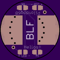
Pilotdog68’s led switch board
Looks like it might have been a problem with your cam job or an odd issue with your eagle. Eagle threw up some errors about your brd file. Re-saving the file seemed to clear the errors. Download the oshpark zip and you can find that version of your brd file inside.
Pilotdog68’s brd file identifies it as 7.2.0
Thanks Helios. What Cam processor do you use? I tried both Matt’s and Oshpark’s and got the same results.
I contacted Osh support and apparently there is a problem with the drills during cam specific to Eagle 7.2. Osh has published a version of their cam specifically for 7.2 and it is working now.
Also, how do you place text over exposed copper pours without osh removing it?
You can’t place silkscreen text on exposed copper. Oshpark will always automatically remove it. You could put text in the copper itself or in soldermask.
How do I add it to the solder mask so just the text is masked?
Just the text masked would be a little annoying to do since eagle doesn’t provide a way to draw positive mask. It would take a bunch of steps but you should be able to do it by importing bitmap of your text. Putting text in copper (positive or negative) would be much easier.
Hmm, how would I do a copper negative?
Create your copper using a polygon then you can write vector text in bRestrict (for bottom copper) or tRestrict (for top). Polygon “orphans” turned on, check box checked in polygon properties.
To create a polygon circle: create polygon triangle, edit one side of the triangle to have a curve of 180 (or –180), delete one of the 2 straight sides, give the last remaining straight side a curve of 180 (or –180). You can now grab and move one end of the circle polygon to change the its size.
I’m considering trying out stencils as manual pasting on larger boards as time consuming… Anyhow, from what I’ve read about stencils you just upload the solder mask layer, but by doing that I get bare ground rings, battery plates and vias included. For those of you that use stencils, do you have a custom stencil project with all the above edited out? Or am I missing something about stencil file generating?
This is what my solder mask for the top layer looks like. I obviously do not want the ground ring, battery connection pads or wire vias exposed on my stencil. How would I best go about dealing with this?

It’s not the solder mask tStop layer. Instead it’s the tCream layer (or bCream for the bottom).
Doh! Of course! Thanks ![]()