Let me be clear: If I were in your shoes I’d use a heat gun to remove the inductor and the FET. The connections underneath those two things are something I’d like to be pretty sure of.
Since I don’t think that’s something you’re comfortable with, we’ve got to beat around the bush a little extra.
Please measure the ohms (200 Ohm range, press hard with your probes on shiny metal surfaces only) on these items:
between the pin on CFC3W which comfychair has marked a “4” next to and the end of the diode with the “4” on it (eg the end with no lines).
there is a cap next to the unmarked SOT23-6. One end is obviously connected to pins 4 & 5 (remember we renumbered this the correct way starting a few minutes ago…). The other is probably connected to pin1 or pin6. Let’s find out which.
If you have not checked between LED- and the middle pin of the FET, please do that now.
1. 00.5 Ohms (as low a reading as I’ve ever got on this DMM so effectively 0 )
2. The other end of that capacitor appears to connect to pin 2 (new terminology anticlockwise w/line marking to the left) which in turn is connected to the bottom right hand leg of the ‘2300’ chip on the other side.
3. I assume you mean the ‘2300’ chip again, in which case this also gives 00.5.
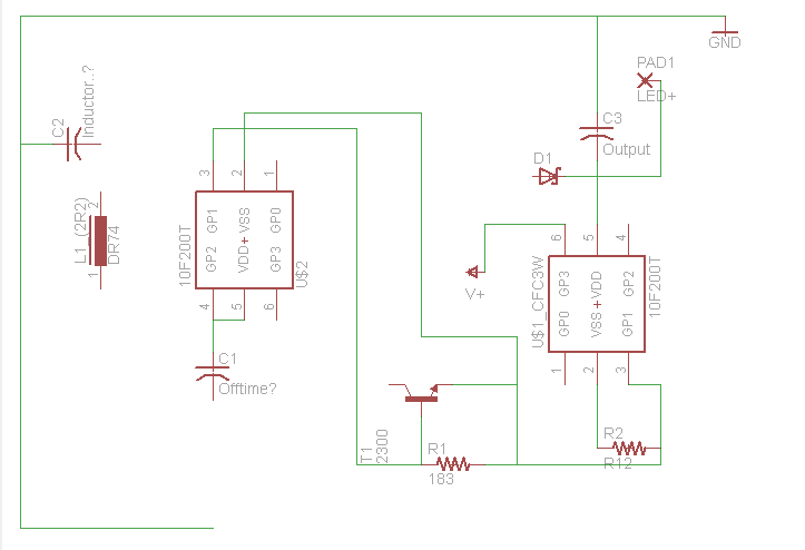
Here is the updated schematic. Note the inductor on the lefthand side with no connections. I just don’t know where to hook it up, and that leaves the function of the rest of the circuit in serious limbo IMO.
Again, good work on your part. I’m just stuck. Right now the circuit I’ve drawn is a DD circuit which won’t function on a single AA. Somehow that inductor hooks up and makes it into a boost circuit. What I’m recommending now is to clamp the PCB in such a way that it is well supported and nothing interferes with (pushes on) the components on the battery side. Then heat it up with a heat gun and pull the inductor. We’ll use the same process in reverse to re-install the inductor.
Sorry for the slow reply again. I’ll give pulling it a go and have ordered a new circuit of similar size in case it goes wrong. Before risking that though I can tell you that the inductor appears to connect to:
1. Battery negative, which connects back through to the right hand side of the tiny ‘R12’ diode on the other side too.
2. At the top side it appears to be connected to the capacitor above in such a way as to feedback on itself through the capacitor.
3. Through the board to the side of the ‘K24’ diode next to the 4.
I’ve checked a good few times and am as confident as I can be about them without actually removing the inductor, which tbh I would give myself a 50/50 chance of successful removal and replacement with, so would rather avoid if at all possible.
Unfortunately the resistance of the inductor is so low that you have no way of measuring what is connected to one leg or the other. That problem is similar to a sense resistor. Case in point: I’m pretty confident that battery negative is connected the left hand side of the tiny R12 sense resistor, but the resistance is so low that you are unable to determine that with a DMM. I’m less confident about the inductor stuff, I can’t just look at it and say how it’s connected.
Before heating the PCB, be sure that you secure it with a clip / clamp / whatever which only clamps to the PCB - not to any components. Heat it up until you see some solder liquefy, then start to poke gently the inductor until you see it move. Once it moves freely you can simply lift it off and remove the hot air. Let everything cool down for several minutes after that before you do anything else.
Ok, I managed it with a jet lighter and some pliers.
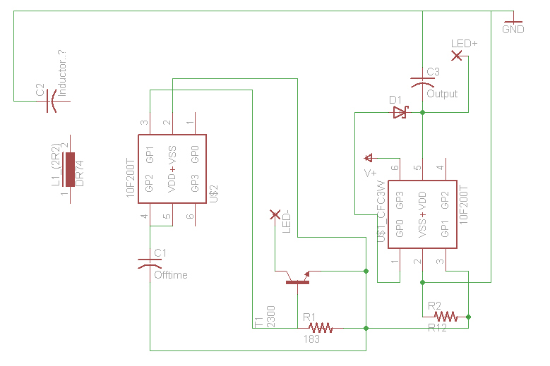
If we look at the inductor as at the base of the board (2R2 written correct way up) then the left hand base is connected through the adjacent gold contact to the top-side of the capacitor next to it, and also to pins 4 and 6 (correct terminology anti-clockwise from bottom left) of the CFC3W chip on the other side of the board.
The right hand base is connected from the trace you can see coming out from under the inductor towards the centre of the board through to the side of the chip marked K24 under the ‘4’ on the other side.
It is not directly connected to battery negative as I had thought before.
It looks good, it can be a little confusing as connections which are close on the actual circuit can be far apart on the diagram and vice versa. I haven’t been able to trace every connection on there but have done quite a few and they all seem to be correct as far as I can tell, I’m not familiar with the presentation though so sometimes I think there is a discrepancy but it may well be just the way it’s drawn in that format.
Are you developing any more well-formed ideas about how the PWM is generated?
Heh, well my current theory is a little embarrassing.
Here’s what it looks like to me right now. The SOT23-6 on the bottom of the board is a monolithic boost controller, meaning that it has an FET built into it. It requires an external sense resistor, external inductor, and at least one or two caps. The SOT23-6 on top of the board is a simple DD LED controller hooked up to the discrete FET (marked 2300) on the bottom. The FET on the bottom has no role in actually creating boost, it is simply present to allow for shutting off the output with PWM in order to produce modes.
If that’s true then pulling the FET’s gate either high or low is all that’s required to bypass the modes… that’s the embarrassing part for me.
The embarrassing part for DQG is that this is a terrible way to implement boost and modes. I’m not sure if the boost controller has a built in voltage limit or if there is some other way that maximum boost voltage is controlled, but typically a simple current-controlled boost circuit (which this still looks like to me) would burn itself up if you disconnected the load. I think.
I reached those conclusions only by studying the schematic. It wouldn’t hurt to compare the schematic with the voltage readings you took.
I colored in one resistor on my lights driver and it made the modes change when the light was simply moved around. I’m guessing that’s what you’d use to disable the modes. Maybe take it out- seems with less resistance it was more sensitive to changing modes. You’d have to have a diagram of the ic that runs it. The way I might do it when putting in the side switch is just use a old 555 timer to do 3 quick clicks and by then a cap fills using the right resistance, it would disable that circuit and run the lamp full out. Kind of newbie way to fix the driver but it should work, there’s plenty of room in the sink.
The pinout appears to be the same as the QX3400 boost controller, which does include an FET like I described. But the QX3400 is a voltage controlled boost circuit while the DQG circuit looks pretty clearly to be current controlled.
It might be possibly to use the QX3400 here if it actually won’t boost past 5v / 5.2v, but I don’t know if it works that way. If it did, I think it might be workable. I don’t think that’s what’s really happening though, because there would be no point in wasting the R12 there. Instead, you’d just connect Pin3 to GND (don’t try that!).
Now, on to more important topics like putting this thing back together. I’d recommend simply reflowing the inductor back into place. If you are not comfortable with reflowing it in order to put it back together, you may have another option depending on space. You can try installing the inductor upside down and using airwires to hook it up. Just be sure that doesn’t make the assembly tall enough to short out against whatever is above it!
I don’t think that this is a side switch flashlight or that there is plenty of space. Are you sure you’re looking at the right light? This flashlight is very small.
Well, I’m not sure I fully understood what either of you were saying, it’s nearly 1am here and tbh I got a bit impatient.
Anyway, whilst bridging some connections on the FET didn’t seem to work, in the end I just pulled it and bridged the contacts with solder. Et voila, single mode!
It seems to run fine, pulling about 1.5 amps on a partially discharged eneloop, which iirc is the same as high was before, so I’m hoping for no burnouts.
Anyway, although the ‘fix’ did turn out to be remarkably simple (I could have even done it without ever removing the circuit!) I would like to say that I am really grateful for the amount of time and depth that you have gone into thinking about this and working it out. It is appreciated to the level of effort and expertise required and applied rather than just the pragmatics of the end solution
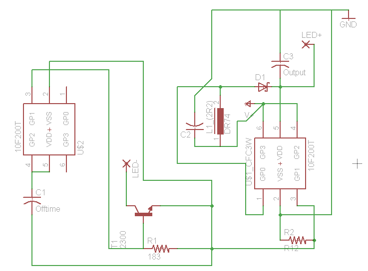
Sounds great. Really that makes more sense. For anyone performing this modification in the future, I’ll change my suggestion. What RedForest UK did is a great way to remove the modes from the bottom. Simply bridge the FET pins marked in blue below. Another option if you take the board out is simply to move the LED- lead over to the two vias which connect to pin #2 on the modes chip - marked in yellow below. The FET (marked 2300), modes chip (SOT23-6, unmarked other than the orientation mark / line), and probably the small capacitor between the modes chip and LED+/- all should be unnecessary after performing this modification - they may be removed or left in place.
Thanks redforest and wight. That worked perfectly on my 15 led Supernight. I just soldered a wire across the fet, then boosted the power a bit with a pencil. Only high mode now. The strobe was pretty annoying to be honest with next mode. I let it run till the battery was dead and it got really hot but it works great
I put a copper scrubber stuft into the head and it does seem to help with lumen loss as it heats up (just a casual observe- no testing done). It seems to stay max bright now for around 30 secs and then starts to drop. Put in copper wire too You saved me the hassle of putting in a 555 timer
Thanks again
Also noticed if you want low mode. You can solder the LED- to here on the fet (pink)
Putting the LED- there just puts a high value resistor between LED- and GND. That’s not a method I would recommend to get “low”. Instead to produce a lower output single-mode you should replace R12 (a 0.12 ohm resistor) with a higher value such as these R900 resistors from Fasttech. R900 is a 0.9 ohm resistor and should produce approximately 100mA output rather than the stock ~750mA output. Use this formula to calculate the resistor value, then pick the closest available value:
sense resistor (in ohms) = 0.095 / amps
So by choosing a value in between 0.9 ohms and 0.12 ohms you should be able to achieve any drive current you want. Note that while I’m suggesting the 0805 sense resistors from FT because they’re cheap and available, the stock one looks like a smaller 0603. This should be fine, there is enough space for it.
I’m really surprised if this is the same driver you have in your 15 led Supernight though. This is a tiny, low-current boost driver. You probably have something somewhat different in your (much larger) flashlight.