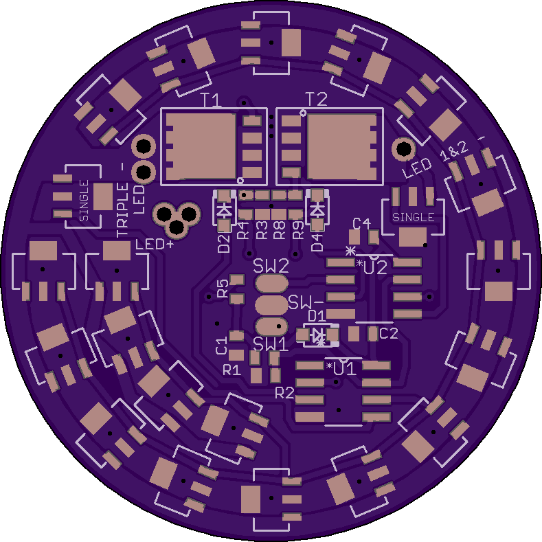
Ok we’ll here’s v01
To do:
Go over it again, it’s an expesive board to find a mistake on 8 minutes after I pay (how it usually goes)
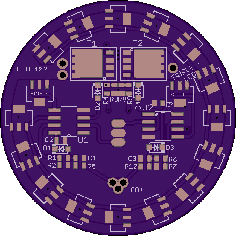
Delete all extra parts TA points out in his post just below this one.
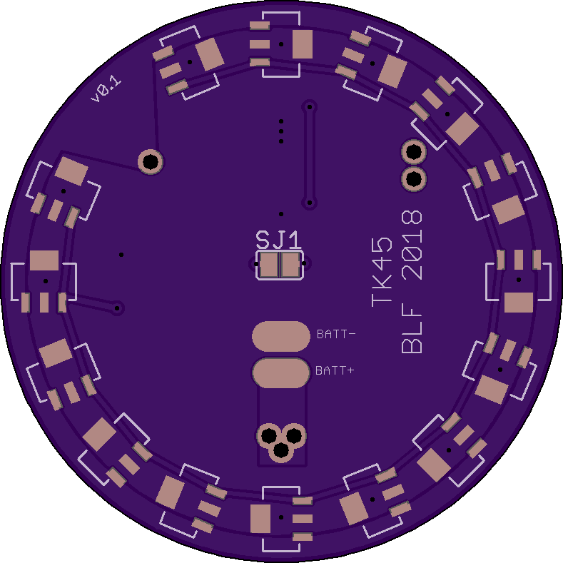
swap to a solder jumper normally closed (that requires being cut to open it) since I expect it to need to be shorted*
Add BLF driver key programming pads for both MCU’s
Move bottom 7135’s in ~5mm for body clearance
*The jumper on the bottom separates the NET connecting the FET’s in case I dont like it IRL.
Next question: What about R10 (R5 in a regular TA driver circuit) and the polarity protection diodes (D1 and D3) can the pairs of those be consolidated into only one of each? Will just one R5 allow enough current to operate both MCU’s?