now that I’m starting on the flashing path (he he), my thoughts are turning to the actual driver. Here are my design goals:
- two separate output channels, each with their own bank of 7135 chips
- both channels controlled by one ATtiny13/25/ etc chip (whatever the footprint is that’s on Nanjg boards)
- through holes for power in and LED +/-. Driver will be controlled by a momentary switch. No mode stars are necessary from my perspective, but if there’s space and they can be used by others, that’s fine by me.
- 6 chip spots per channel (~2.1-2.3A output per LED?) - could be more if there’s space and other users could use them
- ideally single sided for reflowing convenience, but that’s not hard and fast
- ideally 25mm diameter or a bit less. Larger could work too, I’d just have to take that into account in the housing design. >30mm would be tricky.
Basically a master-slave set up on 1 board
Use would be in twin LED bike lights run off 3.7V battery packs. A single board would make packaging and housing design easier and the through holes would make for a much more robust connection - the bar mounted light at least will see alot of vibration and shock. Two separate channels gets around running the LEDs in parallel and allows alot more flexibility in running 2 different LEDs or power level per LED.
Would anybody be able to design this for me? I know it’s a lot to ask and I can’t offer you anything for your time other than my eternal love and gratitude The design would (with the agreement of its designer) be made freely available for download/ printing. I’d love to learn how to do this myself but it took me over a year to get round to flashing my first chip and a month from soldering the programmer to getting a flashed chip, so the chances of me doing this before next winter are pretty slim!
If no one else is willing to I can bust out a simple board in an hour or so…
I’ll try to get to it today (already having an eagle work day), what pin’s do you want controlling the 2 banks of 7135’s? Also what’s the EXACT size you need, also are there any other placement requirements (like say no components taller than x.xmm within x.xmm of the edge of the board). What size spring pad? What pin do you want the momentary switch to go to? You want it to pull that pin low or high?
I’ll start with the easy stuff first - there are no placement or spring pad requirements, although if you can find an electrically neutral pad to put directly under the Attiny chip so I can thermally couple the board at that point to the housing, that would be really neat. Any placement/ spring pad requirements would be dictated purely common sense and by other potential users (if any exist) that would want to stick this in a torch/ flashlight. For my use, it’s going to be secured inside a cavity in a housing that I machine, so I can design the housing around the driver - I really don’t have a handle on what other lights this might go in. I guess it would probably be easier to assume it won’t!
Size - aim for 25mm, go up to 30mm if that allows a single sided board. If there’s space for a 4-40 cap head screw to go through and secure the driver to the housing, that would be awesome. I can measure one with a micrometer when I get home if that helps?
Other stuff - could you use the same pins (and effect of closing the mom switch) as is found on the Nanjg boards? I’ll be using or modifying JonnyC’s/ Toykeeper’s Star-momentary firmware for this driver, so it would keep things simple to use the same pins/ processes as they do.
This pretty much already exists as my SL3_JohnnyMac edition. Just need to size it down very slightly. I started fresh…
I do still need to know what exact pin you want the second output to be. I’ll check the datasheet to see whats’s alailable as far as PWM capable pin’s, if there’s only one other that’s simple, if there’s a third you’ll have to choose.
What are you trying to do? I have a PIC driver that does this already for tint mixing. Uses 2 banks of 7135’s (plus a third common PWM that goes threw a set of BJT’s to make the mixing work better). Probably does more than you need tho and not AVR. Not trying to talk you out of this or sell you mine- it’s not ready for sale yet anyway, just curious what modes / UI this will have needing the 2 channels.
ah right, I’m getting the confusion. Aim is to run both channels off a single pin - both will receive the same PWM signal from the driver, both LEDs will be lit at the same time and the same level. What I want to do is a simple master-slave driver, ie. use 1 ATtiny13/25 etc to drive 2 boards, each LED being driven by a single board, but do it on a single board. I don’t want to do anything funky with the 2 channels (any difference in drive current could be crudely set by the no. of 7135 chips). Essentially, I could do this using a Nanjg board and separating the traces for LED- between 7135 chips 4 and 5 so that I could wire up an LED to each bank of 4, but it would be fiddly, not terribly robust and nowhere near as cool. That’s why any of the existing Attiny momentary firmwares (or even the clicky ones, really) should port right over, I’m guessing?
Oh ok, I thought you wanted something like I’m doing where you can control the 2 LED’s individually (or like Wight’s project here where he uses 2 different PWM output pin’s).
Ok that will be even easier, no problem either since I havent routed it yet, just have to move one connection in the .sch. Will be done shortly.
@mattthemuppet
you can do that with ordinary NANJG 105C, just add some chips if you need and cut some traces, someone already explained which trace to cut but I can’t find that thread…
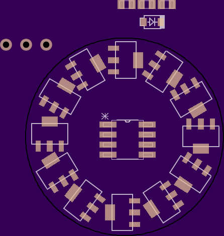
There's 2 LED+ 1.1mm via's, the 2 LED- 1.1mm via's a .8mm SW+ via and then left tinted is a 1.1mm GND via for hooking up to your contact board / setup. I could make it 25mm but there will be almost no border around the ring of chip's, 26 is a pretty common size in Chinese lights so i went with that. Let me know what changes (if any) you need, bigger spting pad or whatever else you want.
that is so totally awesome I’m temporarily speechless . . . . ok, speech is back! Wow, can’t believe you did that so quickly, that would have taken me months! So very cool.
Right, now my jaw is back up where it’s supposed to be, a few small queries:
1) 1.1mm vias for LED+/- = ~18awg, right? That should be more than enough at those currents
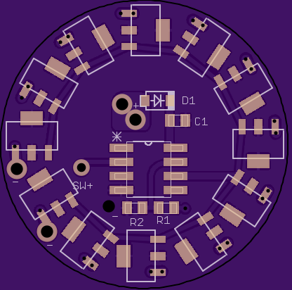
2) would it be possible to put a large electrically isolated pad in one the open spot to the top left of the Attiny chip, with vias linking both sides of the board, and a 3.1-3.2mm hole in the middle of it? Purpose would be to have a spot to bolt the driver board to the light housing (using a 4-40 or M3 screw) to thermally couple the driver so that the temp sensing on the Attiny25 chip reflects LED temp as closely as possible. It’ll also make it really easy to mount and remove the driver, if necessary - something that’s not the case with the Taskled drivers. Electrically isolated so I don’t have to fret too much about risk of shorting anything through the case.
3) could you move D1 and C1 a smidge to the right and add a third positive hole to that LED+ area? Then I can wire in Batt positive (as well as LED+ 1 and 2) from the top, instead of underneath
4) would it be worth putting Batt negative up to the right, between C1, Attiny and the 7135 chips? It’s all the same plane electrically I think and it would leave a wee bit more space for soldering (does it need a solder pad too?). Perhaps put a SW negative pad/ via in the same area too, just for ease of use? Then everything can be soldered in from the chip side, which will make wire organisation a lot easier.
I’m so pumped by this!
Gotta go and finish a lecture for tomorrow, so might not get to see this until tomorrow afternoon (I teach from 8-12). Thanks again!!
totally! The main issue that I was hoping to fix was actually the through holes for soldering. I figured while I was at it, there was no harm in getting a few other wish list items too
I know that this has now been nixed, but for reference that driver uses Pin5 and Pin6 for PWM. It also uses Pin3 and Pin1 without PWM, but Pin1 is definitely the last one you want to use if you can avoid it. It requires special hardware to reprogram a driver after programming it to use Pin1.
AFAIK the convention is to use 8.4v packs for bike lights, not 3.7v packs. Since you’ll be running two emitters (XM-L2 / XP-G2 or similar I assume, eg 3-4v each) it would be easy to wire your light up to run on 8.4v packs. This will cut your need for 7135’s in half and cause you to need one extra resistor and a Zener diode. Have you considered that option?
the main reason for a 3.7V pack is ease of construction and charging - the 2S and above packs I’ve made have balance wires+plug to help pack longevity and don’t have PCBs, largely because I’m tight and high drain 2S+ PCBs are about the price of a cell or more. So making the packs is a bit of a hassle, they can be tricky to seal well against the rain and I have to drag out the hobby charger to charge them. With a 3.7V pack construction is a piece of cake, there are plenty of high drain single cell PCBs around, I can add however many cells I want instead of doing them in multiples of the voltage and charging is simple. I’m even thinking about how best to add and waterproof one of those cheap miniUSB>li-ion charger boards that I’ve used on a bunch of lights, which would be the ultimate in convenience!
Plus this approach should make driver construction that little bit simpler - all one would need is a Nanjg or two and a soldering iron, no extra parts required. Not a big deal for the majority of people on here, but a small plus nonetheless
C_K is indeed awesome, no doubt about that!
Can’t answer to the diode thing, but the lack of ground ring is I believe to keep it small yet still allow it to be used in a torch/flashlight with a battery contact plate.
Oh, there’ll be a lot of pics, that’s for sure! I’ve been thinking and thinking about this build for nearly 2 years and it’s gone through several iterations in that time. Just remembered, another thing that I want to get down for this build is anodising, although that should be simpler as I have all the components but haven’t had time to try it out. It’ll be a pretty kick bum little light - 2 XM-L or XP-L, running around 1.7A each behind 10deg optics, 3 modes, 2S battery on the helmet on a quick release mount, remote switch attached to the helmet. It will take me a long time, but I’ll get there eventually!
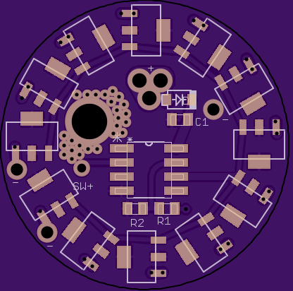
I’m not sure about bolting it to a metal housing, that seems like its going to cause shorts. The thermal via’s and large mounting hole (3.2mm) are isolated but I dont see how you’ll bolt that down to something and not have the + via’s short out.
Is this what you need? If not I can make a few more changes.
looks fantastic and no need to apologise at all - I expected this to take weeks, not days or hours!
a few small tweaks if that’s okay? I don’t want to take up more of your time than necessary.
1) could you move B- down a touch, say so that the bottom of the solder pad is level with the bottom of the 1 in C1? Just to provide a bit more clearance from the 7135 chip it’s next to.
2) those thermal vias look awesome and that mounting hole will be super useful. Could you however remove the vias that are close to SW+ and the top left pin of the ATtiny chip please? That would remove any risk of getting solder whiskers bridging the gap. The idea for the mounting pad is to have a raised pedestal that extends under the Attiny chip that the driver will be bolted to, that way none of the wires in the through holes will be able to short. I think George at Taskled actually sold little machined bits for people to do just that with their B2flex drivers.
3) could you put in a SW- via and solder pad please? Somewhere south of B- in that little pocket would be great! Could you also move the SW+ a bit further down into that pocket too? So that the trace slopes down to the left? That would free up a bit more space around the mounting pad for the pedestal.
4) is there enough space between the 6 o’clock and 7 o’clock 7135 chips?
I think that would be it, unless anyone else has any comments? Thanks again!