Here’s a 24,000 lumen high bay light for around $1100US at Grainger.
Cool bin so contrast before CRI , nowhere with electric wiring work.
Foundry quality control,or press/forge shop.
Runway light?
Yes! That’s where it’ll be mounted to replace HID lighting.
Correct, its a hi-bay!
It sure is!
Bingo! Its made my Holophane and the model is the Phuzion. The brand is wrapped under the Acuity Lithonia group. The model you linked shares the same head as mine.
Here’s a sales brochure PDF and a link to the photometry report for the lumen dispersal from my model.

They are found there too! Interestingly, a heavily televised hockey sports arena (dont remember which one) upgraded from HID to these to reduce their power consumption, add programmable dimming capabilities and add CRI to the playing field. Going from 50 CRI to these produced the results they wanted while adding definition to the rink.

Thermal IR

Wow, very cool! I guess for $1100 it should be thought.
Strange saucer shaped things with lots of bright lights ![]() .Now where have I heard that before?
.Now where have I heard that before?
Congrats on figuring out what light the image in the OP belongs too. Does that mean DavidEF gets the light for free now?
FlashPilot wrote:
DavidEF wrote:
ImA4Wheelr wrote:
Anyone see any signs of thermal pads under those emitters? They appear to be 119’s.
There are thermal pads. Look at the thin raised track running straight through the centers of the emitters. That looks to be the thermal trace.
219B’s. Great deductions and a good eye, sir.
That trace arrangement doesn't seem likely. Both the 119 and 219 have the electrical pad going up long the sides with the solder blobs (In the OP image). For instance, this O-L image of an older 219, you cans see how the markings on the top of the emitter align with the electrical contact pads.
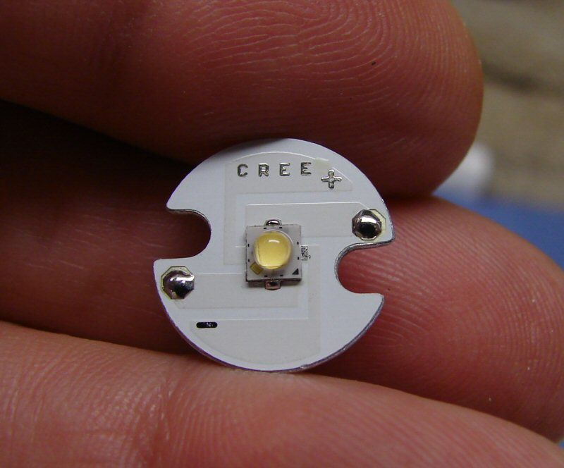
I'm not saying the emitters are not 219's. It would make since that the big traces that DavidEF thought were electrical traces were actually traces for spreading heat though. But if they are, they did a very good job of not using any excess solder for all of the visible thermal pads. Unlike every other pad in the picture in the OP.
Ack! In China, Confucius say, “better to have waaaaay too much solder than not enough.” ![]()
From casual observation, its typical not to see any solder visible around the emitters/SMD’s on many high end production builds. Its the difference between what was produced by an ISO 9001 certified automated production giant employing expensive modern process equipment, versus something that was slapped together by cheap unskilled labor using whatever was available to get the job done at the absolute minimum expense (which is why their builds are never consistent and suffer far higher failure rates).
I also own a GE Evolve LED light array (which also sold for $1100). As expected, none of the XP-G’s in that unit show the slightest hint of solder attaching the emitters to the mcpcb.
A huge part of ISO standards relates to uniform precision production, detailed documentation and audit trail, which is why the Holophane rep was able to tell me all the fine details of the build. The only reason I called them is so I could order the same emitters to reflow my own in case one or more failed in the future. The populated replacement board by itself was a horrendous $150. :Sp
$150/112 = $1.34 per LED? Doesn’t seem like a bad deal, maybe you can do some harvesting after all ![]()
I think FP mentioned there are 4