Specification:
Changes are highlighted in bold
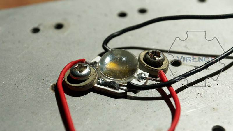
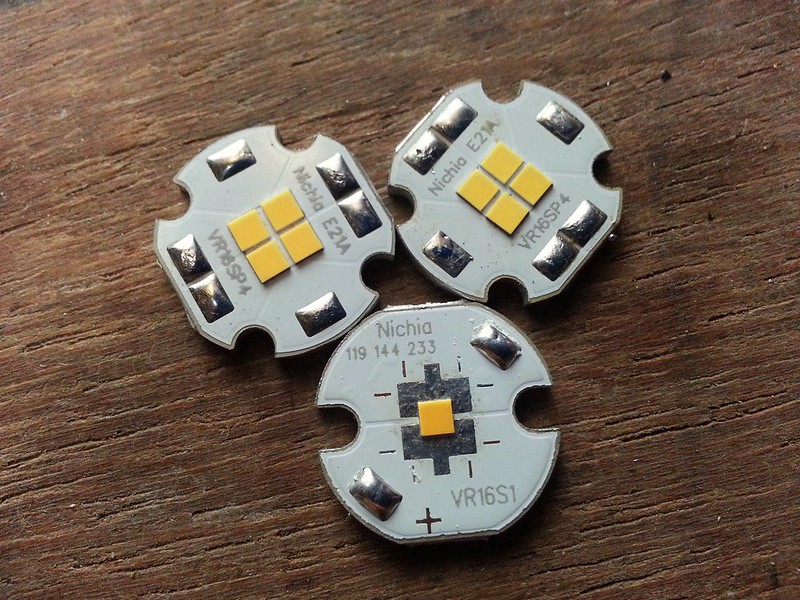
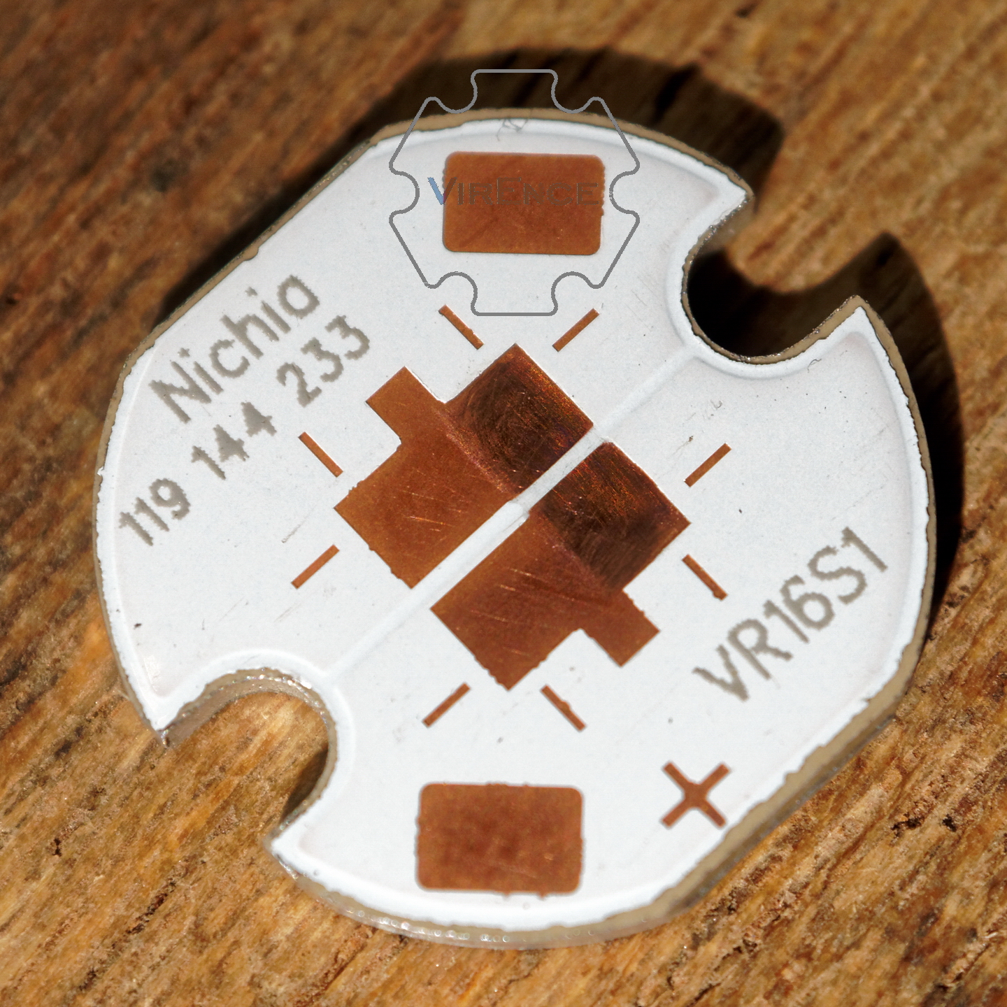
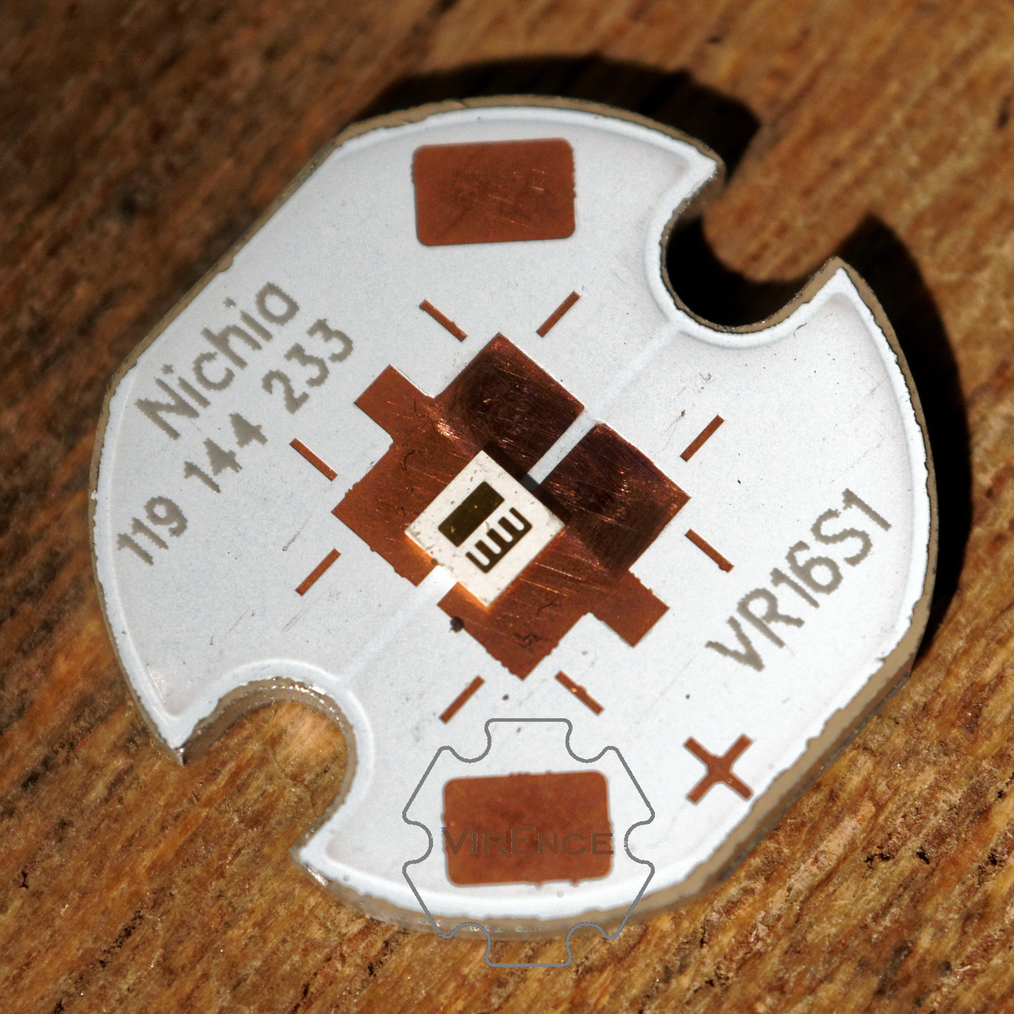
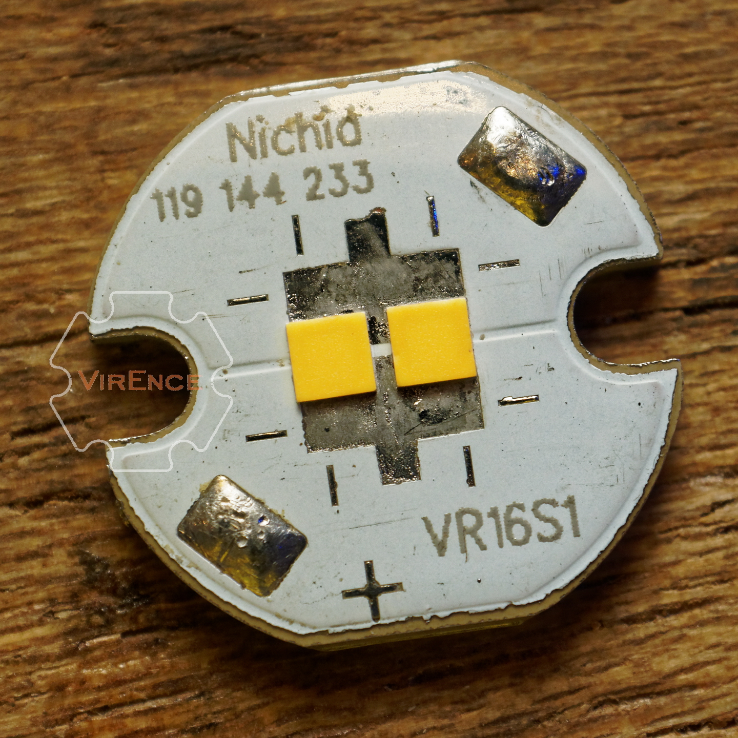
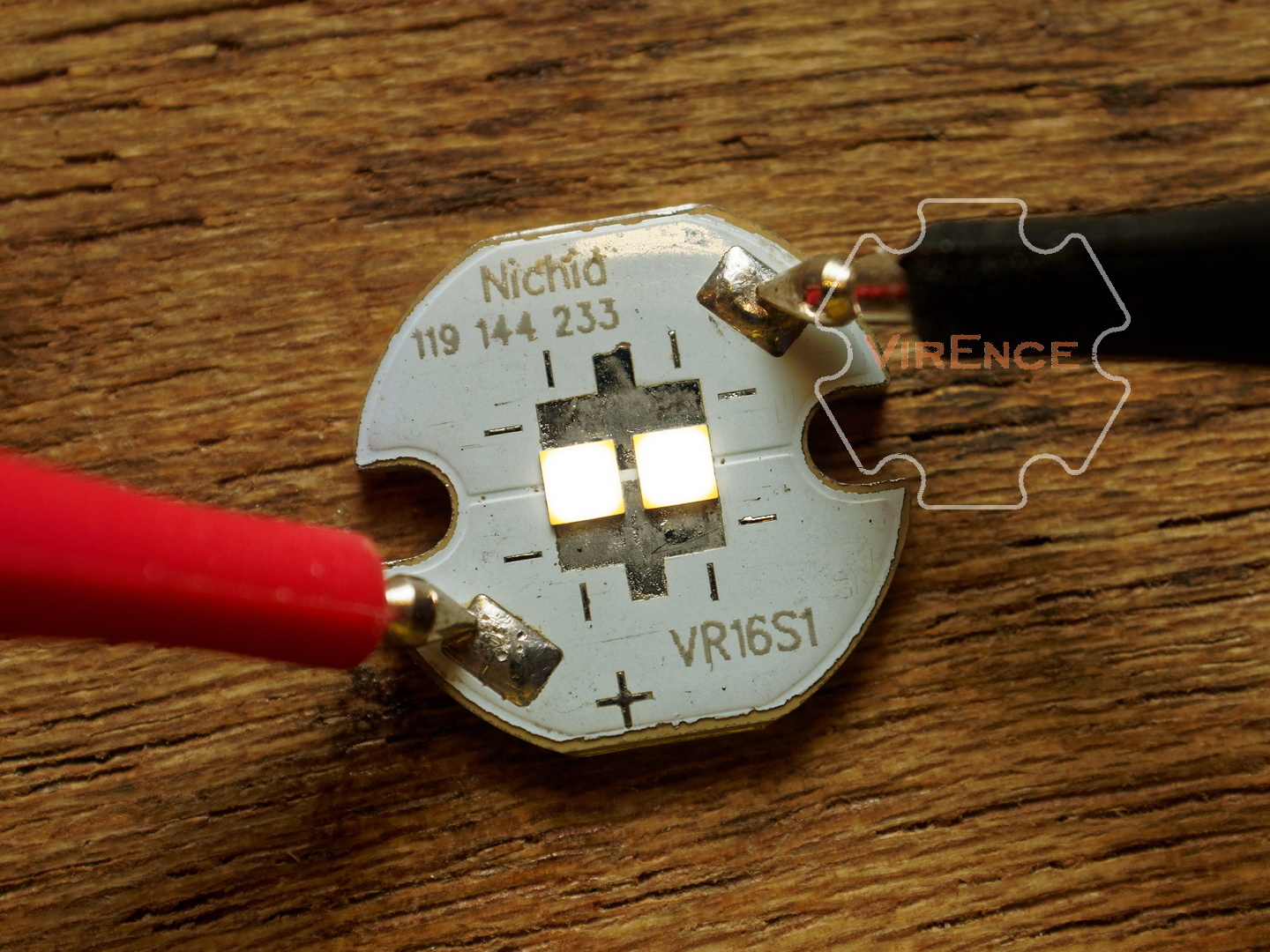
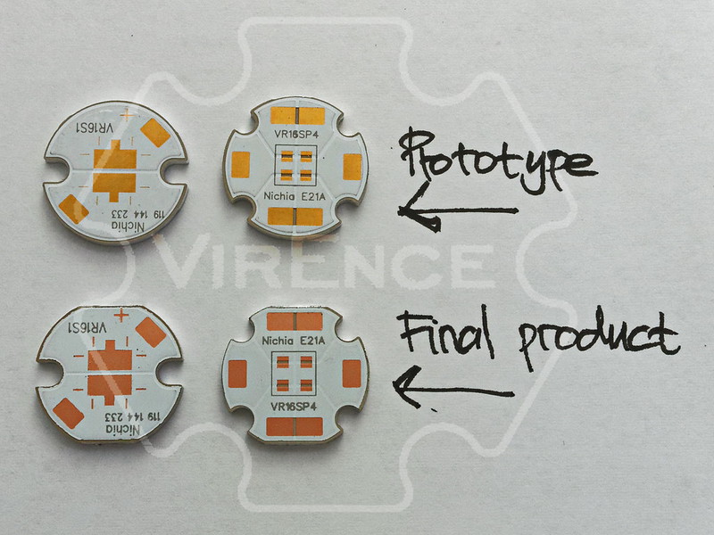
VR16S1
- MCPCB thickness: 1,65mm ±0,1mm
- Dielectric thickness: 10µm ±3µm
- Dielectric thermal conductivity: 7,5W/MK
- Copper trace: 70µm
- Solder mask thickness: 15µm ±5µm
- Anode - cathode gap: adjustable from 0,5mm down to 0,2mm (was 0,5mm to 0,3mm) by scraping off the masking
- Brighter reflective white solder mask
- Tougher solder mask (untested): prevent yellowing in sustained leadfree 260C environment.
- Copper pads plating: OSP (was ENIG) to get every last bit of thermal performance
- Flat section for V-scoring 15mm maximum (was fully round): mass production consequence
- Routed MCPCB’s outline, not punched to get the flattest possible bottom.
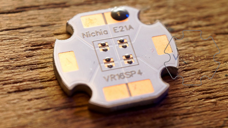
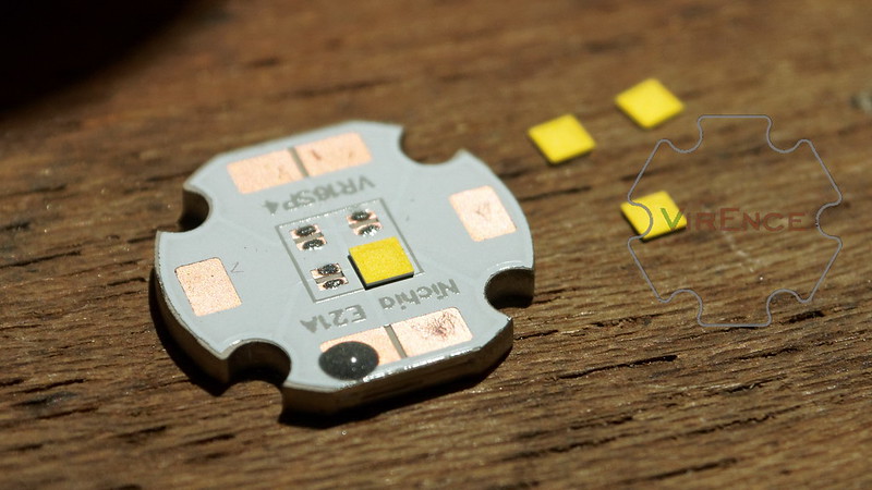
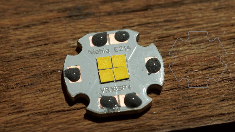
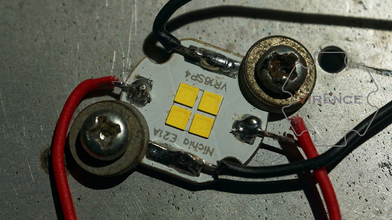
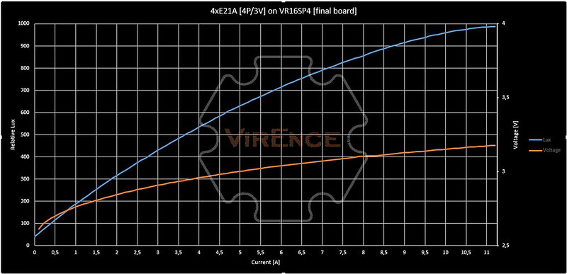
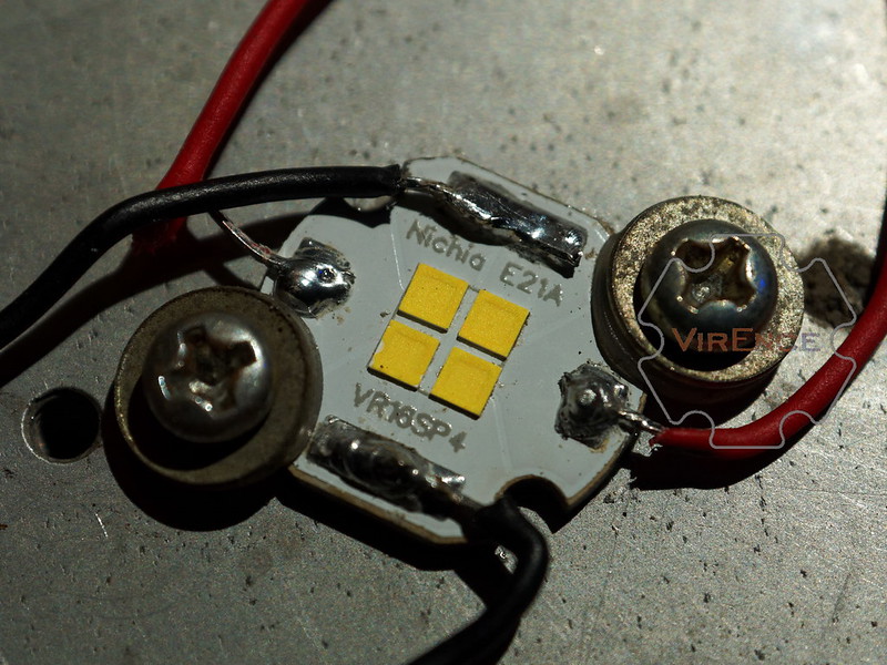
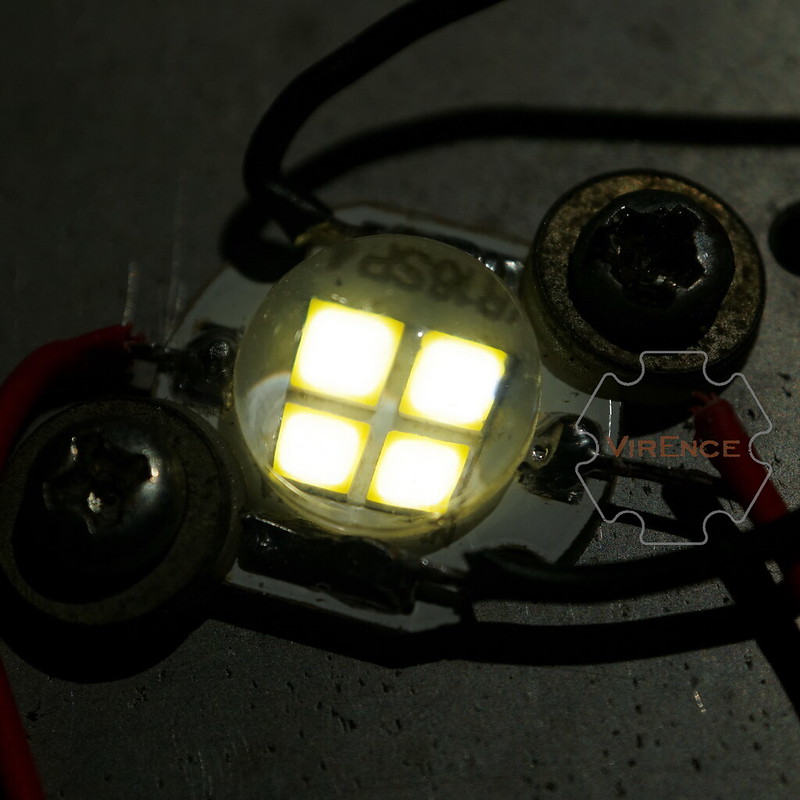
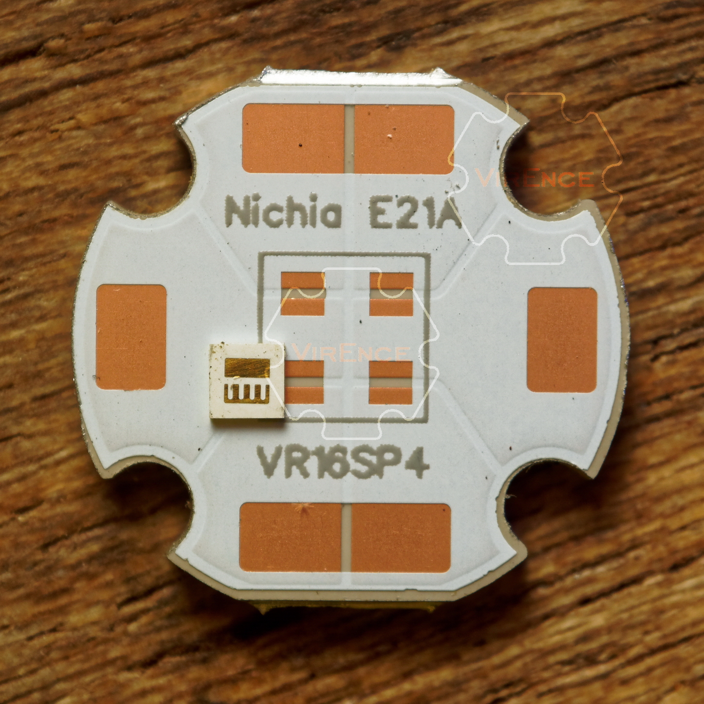
VR16SP4
- MCPCB thickness: 1,65mm ±0,1mm
- Dielectric thickness: 10µm ±3µm
- Dielectric thermal conductivity: 7,5W/MK
- Copper trace: 35µm (was 70µm) for better reflow process
- Solder mask thickness: 15µm ±5µm
- Anode - cathode gap: 0,2mm (was 0,3mm)
- Final quadtrix footprint: slightly adjustable from 4,4 x 4,4mm to 4,6mm x 4,6mm (was 4,2 x 4,2mm to 4,4 x 4,4mm).
- Brighter reflective white solder mask
- Tougher solder mask (untested): prevent yellowing in sustained leadfree 260C environment.
- Copper pads plating: OSP (was ENIG) to get every last bit of thermal performance
- Flat section for V-scoring 15mm maximum (was fully round): mass production consequence
- Routed MCPCB’s outline, not punched to get the flattest possible bottom.
- Clemence