Hi guys,
I'm going to make custom copper round CDTP MCPCB for a single Nichia 144A.
This new board will have several features:
- Non insulated for superior heatsinking with direct soldering OR Insulated with options to use either thermal adhesives or pad
- High reflectance white masking ink
- High temperature masking ink (lead free/direct soldering friendly - less yellowing)
- Hopefully will performs same or better than my previous 30mm x 30mm VirEnce board (will post the test result later)
The sneak peek of the design is in my avatar. The questions are:
- Diameter (tell me your favourites, could be more than just one size)
- Thickness
- Optics (tell me your favourites, could be more than just one type)
- Slots? (most used cable thicknesses)
Please post your suggestions. Thank you!
May the Photons be with us,
Clemence
-----------------------------------------
Update 170913:
I finally able to start the project. Thanks for all the support guys.
After many hours of sketching and discussions with some BLF brainiacs, I sent the final models up for prototyping today. The process alone will take 4 weeks, excluding shipping and document preparation. I'll report when I get the first 60 pcs of sample later.
Below are the two models undergoing processing:
16mm 5050 footprint quad [E17/E21 only] configurable for 3V, 6V, 9V, and 12V
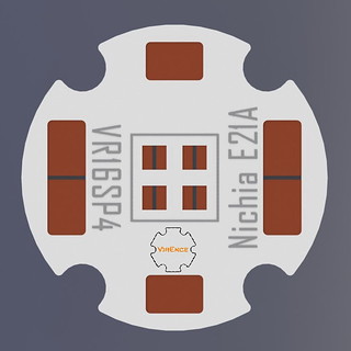
16mm single [E17/E21/119/144/233]

--------------------------------------------------
Update 171016:
- 60 pcs prototypes shipped!
--------------------------------------------------
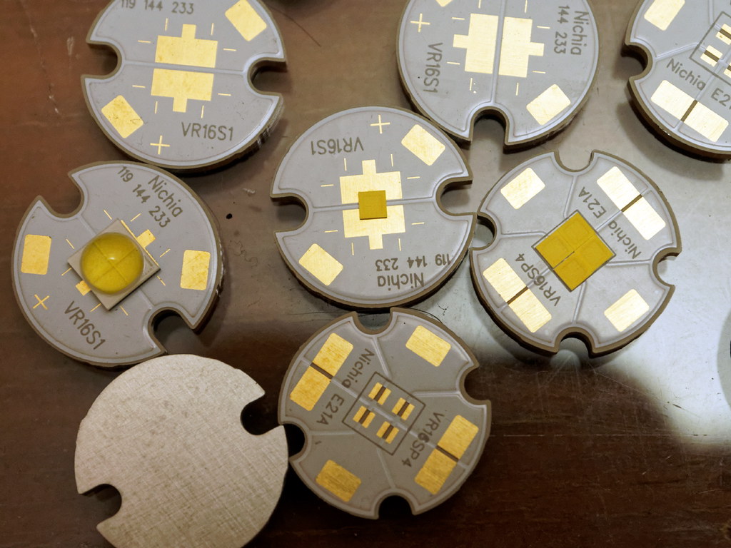
Update 171025: Finally the first prototypes received.
These are the most ultra EXPENSIVE MCPCB I've ever had. Here's the preview:
-------------------------------------------------
Update 171026:
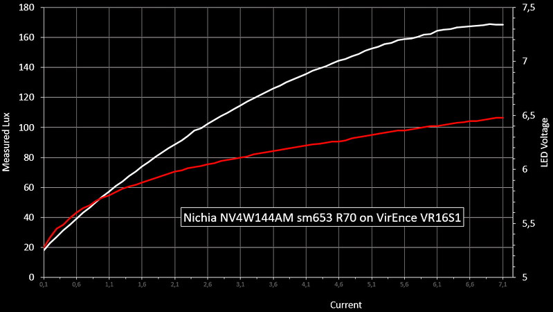
Hooray! New record for 144AM.
The new TINY Aluminum NON DTP 1,5mm thick 16mm VR16S1, beats my older bulky 2mm thick 30mm x 30mm (CDTP copper).
This is a great achievement!
Peaked at 6,9 - 7,1A & 6,48V (shallow decline after 7A). Previous record was 6,4A & 6,2V (way hotter and drops rapidly after peaking). The quick test up to 8A didn't kill the LED yet. I didn't measured it since it's already dropping down, and was too excited that I accidentally moved the lux meter position. It must be brighter since the LED vF was lower.
I never thought the result would be even close to the early test. I couldn't measure the lumen output but the lux curve and voltage reading is a valid data to conclude this.
Early test by Djozz:
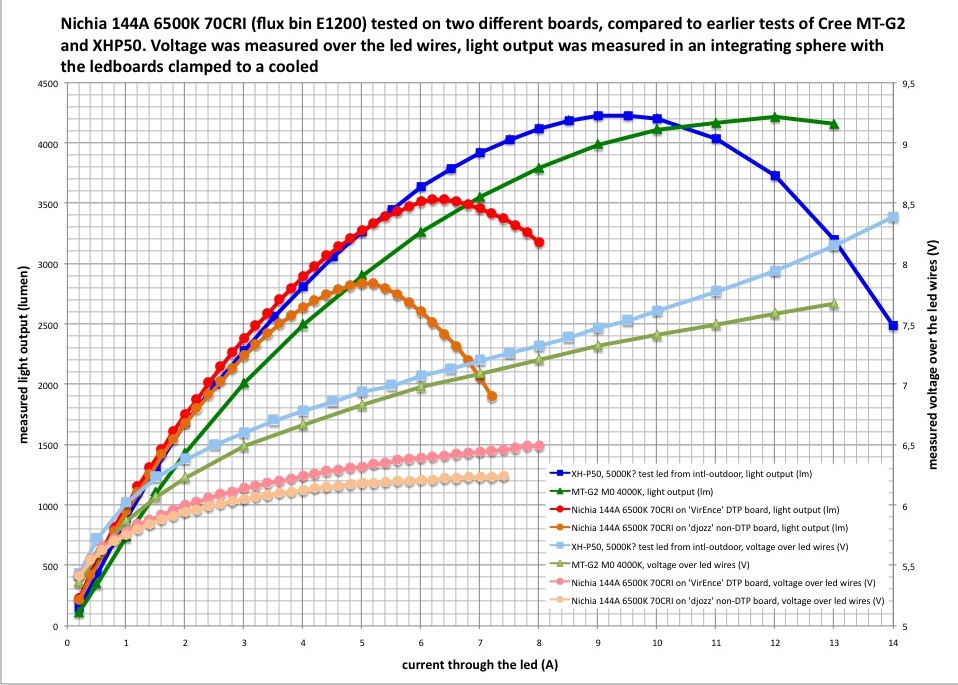
Almost 50watt of raw output. My estimation based on Djozz's test, this new board is capable to bring 144AM/AR E1300 R70 to output close to 3700 Djozz lumens and 3000 Djozz lumens for the R9050. The correct voltage shown by the DMM in the right.
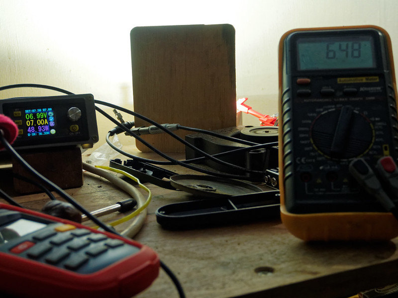
T-connections to measure LED voltage
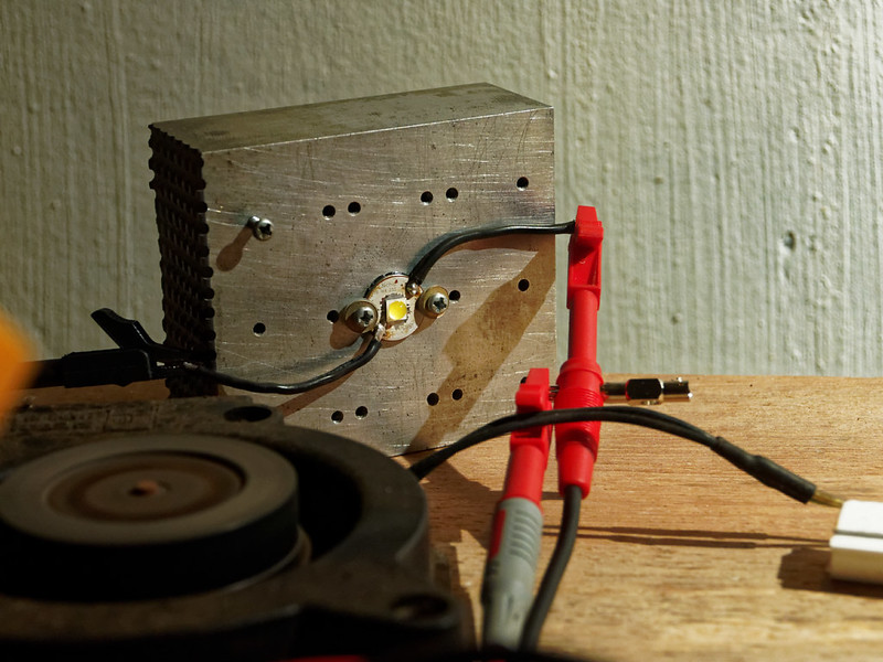
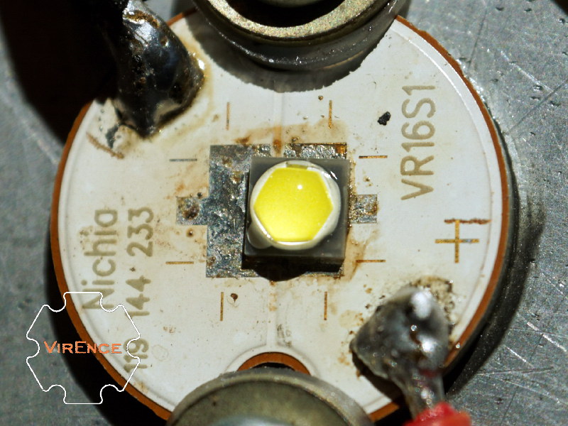
The poor guinea pig undergone many reflows and scrapings. The solder mask is indeed very thin and fragile. I asked for it to create the thinnest bump possible between pads. Even though the solder mask is fragile, the super thin 20nm (nano meter) dielectric withstands multiple 260C reflow cycles successfully with no delamination at all. Wire soldering was rather difficult due to excellent thermal dissipation. I abused my 30 - 200 watt solder gun extensively to create simple wire joint. It's like soldering the thermal pad of DTP boards.
The board mounted using only Moly-graphite automotive grease and two M3 x 0,5 screws.
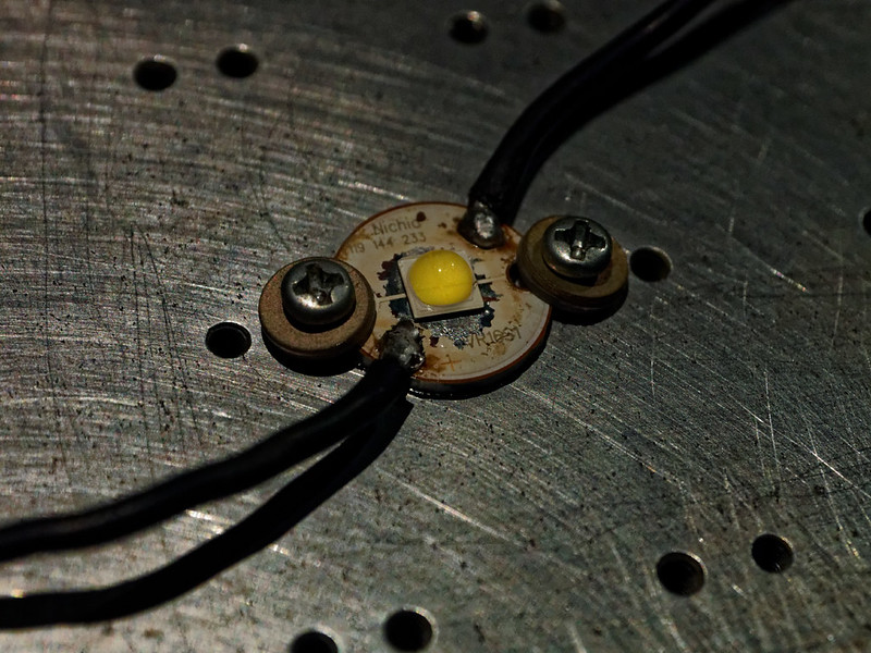
That's all for today. Tomorrow I will test the quad E21A.
--------------------------------------------------------------------------
Update 171027: E21A single and quadtrix test results
Here's how to convert the VR16S1 to fit single E21A. The gap between pads was 0,5mm. By scraping the solder mask using sharp artists knife you can get 0,3mm gap. I asked for 0,2mm but the 2 oz. copper trace makes it difficult to maintain close tolerance. The test sampling from the manufacturer resulted in 2,9 - 0,31mm gap. Let's hope the next production stuff can make it closer to the target 0,2mm (+/- 0,05).
I used polyimide high temp tape (similar to Kapton tape) to keep the LED from twisting during reflow. You can see later in the picture that this tiny E21A is very prone to twisting. And the result was uneven heat spreading across the tiny thermal pads. I learnt that next time I must place the tape at the cathode side. E21A has different anode - cathode design. The cathode has larger surface area, hence stronger solder adhesion during reflow.
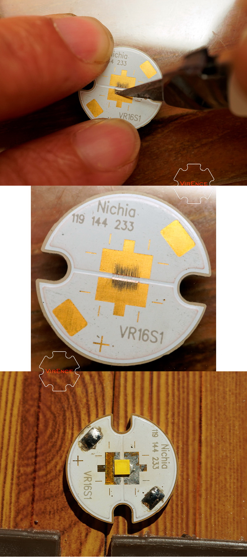
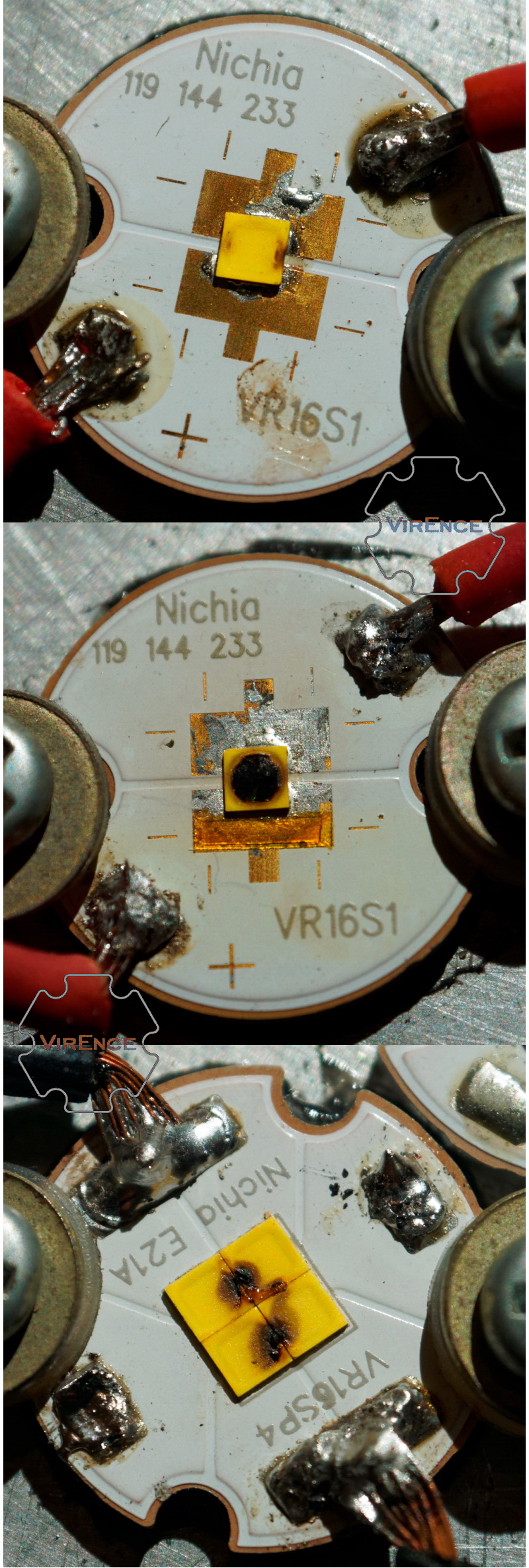
Various deaths of E21A:
top: twisted uneven thermal load between anode - cathode resulted in burnt phosphors started from the side. EDIT 171104: any slow death always started by side burns. The only path to cool the phosphor/silicone protective layer are: air and the die.
middle: good centered LED resulted in burnt mark started from the center (the hottest point) EDIT 171104: Quick current sweep to the known maximum resulted in center burnt mark. This happens because the phosphor and silicone protective layer still relatively cold at the sides.
bottom: combination of dirty (non visible at first) LED caused by burnt flux residue, recycled E21A's from previous reflow attempts, and of course tightly packed matrix. EDIT 171104: In cramped gapless config, the burns always start in spots farthest from the anode and cathode in the boundaries between LEDs. The crossing photons heats the neighboring LEDs.
I expected the problem when I check the board after reflow. I saw oily substance creeping out from the seams. Cleaned it with IPA but later during the test, the smoke was visible even at 1A. The trapped flux, liquify at high temperature and narrow gaps between LEDs acted as the capillary path.
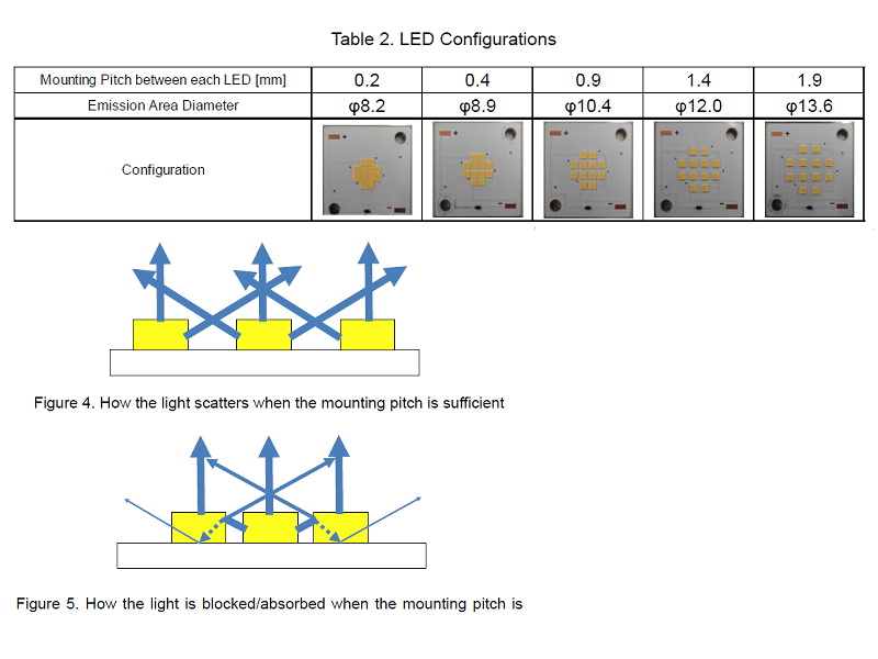
The only cure is to open up the space farther. I plan to make at least 0,4mm gaps. It's needed to prevent trapped flux and photon crosstalks. The benefit of better beam shape isn't justify the reduced capability. Please keep in mind that VR16SP4 isn't designed for thrower. The beam pattern behaviour could be like those in XHP50
Here's why the phosphor doesn't have regular thermal path like "normal" LED. Usually the phosphor sits on top the AlN or SiC substrate separated only by thin reflective layer. The thicker silicone coating also aids in photon extraction better (less heat buildup)
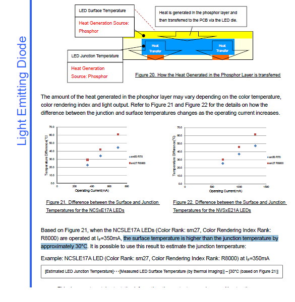
You can see that even at very "low" 350mA current the phosphor already 30C hotter than the die. No wonder it got burnt way faster than the die. Above example are using generic performance MCPCB. The only thing we can do is to reduce die temperature as low as possible and prevent any unnecessary photon cross talks (by opening the gaps).
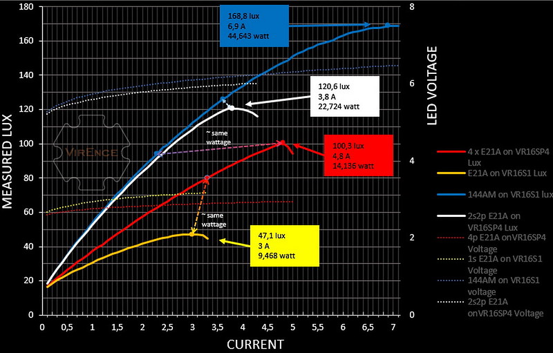
And here's the combined chart:
CONCLUSIONS:
- This board is an excellent choice for many two pads Nichia LED such as 144, 119, 233 and could be used with many other brands too. The performance, in my opinion is very close and COULD even better than any DTP boards (2 pads LED has more exposed total area/footprint ration than 3 pads LED). I will try to test 119 and 219 LEDs using both VR16S1 and any decent copper DTP later.
- E21A maximum drive current doesn't significantly improved by the low thermal resistance of these boards. Only 200mA higher than common copper MCPCB in VR16S1. The brightness below maximum current and lower junction temperature are the most interesting gain to be expected.
- E21A maximum drive current is limited by the phosphor temperature. As can be seen from my earlier test (the Twig-light thread) with the burnt phosphor/encapsulant (the white reflective silicone blanket) removed, the bare blue light output increased steadily to ~ 6A region.
- The quadtrix board VR16SP4 could be improved by opening the gap further to 0,2mm between LEDs to make reflowing easier. Now the total footprint is only 4,2mm with gapless version, still plenty of (0,8mm) margin to make it compatible with many 5050 optics. I will test it again using clean fresh LED later.
- Watt per watt, the quadtrix E21A efficiency was higher than 144A even tested using "dirty" used E21As. I tested using the highest binned LED: D320 for E21A and E1200 for 144AM
- in single setup E21A max drive current was 3A. I expect something like 8-9A total in a proper 4p (VR16SP4) config.
- In 4p config in VR16SP4, the voltage for each E21A were very low. I think this is the combination of less resistance (Ohm's law) and hotter junction temp. The lower voltage recorded consistently across the current range (0,1 A - 3,3 A)
- There's no point in using single E21A in most applications higher than 0,2A / LED (if luminous flux is what you're after). You can see from the chart above, there was HUGE efficiency and output gain by using 4p E21A compared to 1s E21A (~ same wattage).
I will make another test later and revise the above points if they're not relevant anymore. Meanwhile those are my latest findings.
-------------------------------------------------
Update 171107: some more tests and comparisons
For those curious about how the good old XPG performed on copper DTP....I couldn't find any XPG tested on copper DTP in BLF.
You'll also find how technology has gone very far back from 2006 to 2017.
First: the LED - much lower voltage yet almost twice as bright (more than twice if I were using newest Cree)
Second:the MCPCB - LED with thermal pad is not as critical as before for most normal applications
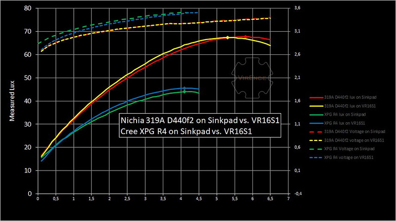
Those test performed rather unfair but should give you the idea. With dedicated "two pads" LED such as 119 or XBD series the result will be much better. FYI, VR16S1: 2 Oz. copper; Sinkpad: 1 Oz. copper.
The result with 319A D440f2 on DTP peaked at slightly lower current (5,75A) than what Texas_Ace did (6-6,25A). This, I believe due to the extra hot tropical temp (tested in 30-32C, 88% humidity).
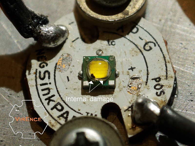
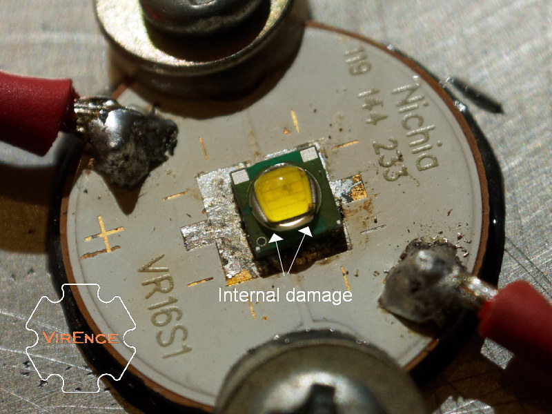
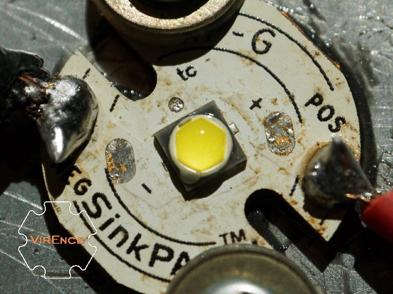
Below are the LEDs after the test:
CCT mixing test results:

------------------------------------------------
Update: 171223 Some excellent tests from Godamn city performed by Rob-inn (Badman's equipments).
https://budgetlightforum.com/t/-/42898/127
https://budgetlightforum.com/t/-/42898/140
https://budgetlightforum.com/t/-/42898/145
and he said there are more to come....
------------------------------------------------
Update 171226: VR16SP4 CCT mixing test result
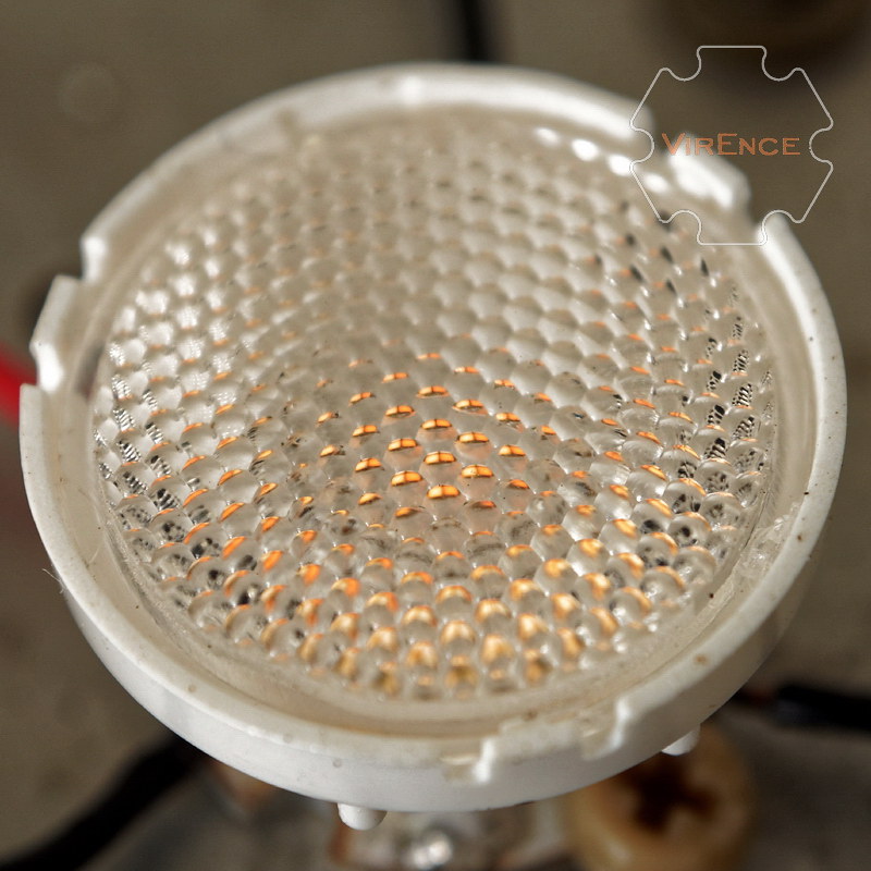
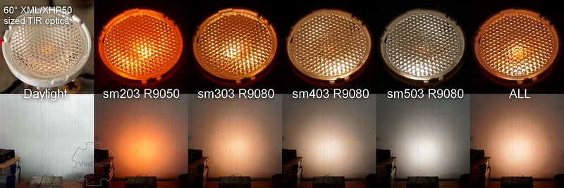
------------------------------------------------
Update 180119:
Latest test for the production VR16SP4:
https://budgetlightforum.com/t/-/42898/168
------------------------------------------------
UPDATE 180706:
New variants, VR21SP4 (quadtrix E21A) and VR21P4 (quad Optisolis/757). Same board material and technology as previous one.

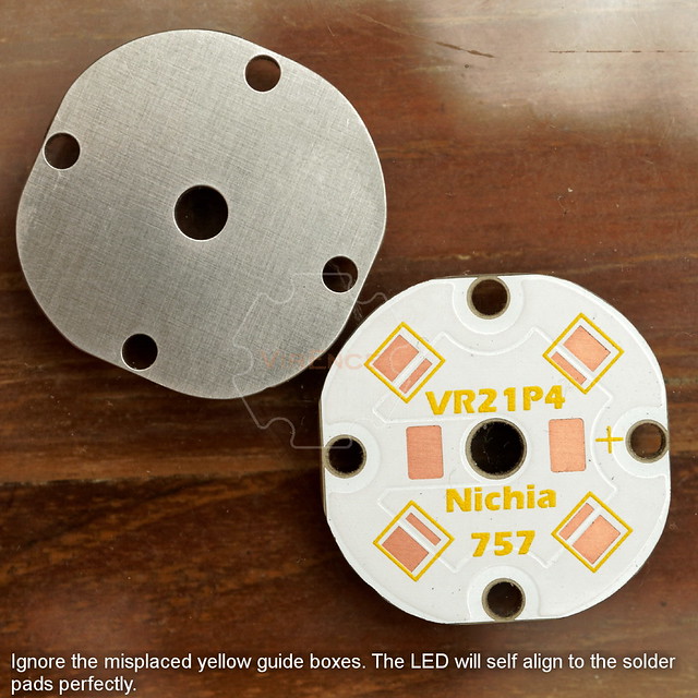
https://budgetlightforum.com/t/-/42898/225
-------------------------------------------------
UPDATE 191104
New MCPCB
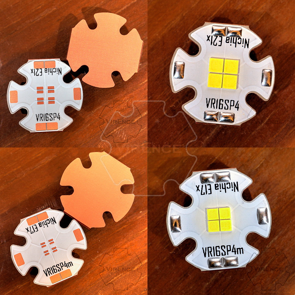
Detail: https://budgetlightforum.com/t/-/42898/320
- Clemence