Matt…can you put V1.1 back on as well as V2.0 on OSHPark…or do you think V2.0 is better?
I still think they are trying to troubleshoot the V2.0 with the pulldown resistors…none of my boards are programmed as I busted my daggum SOIC clip so I can’t program anything…so I can’t test or anything…uggh
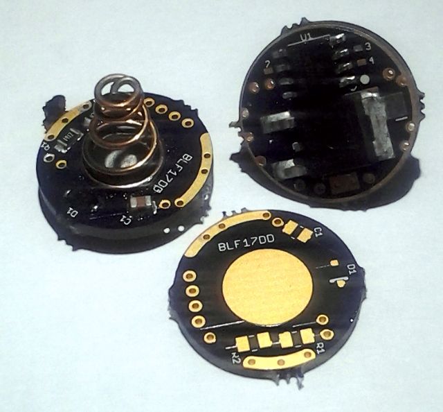
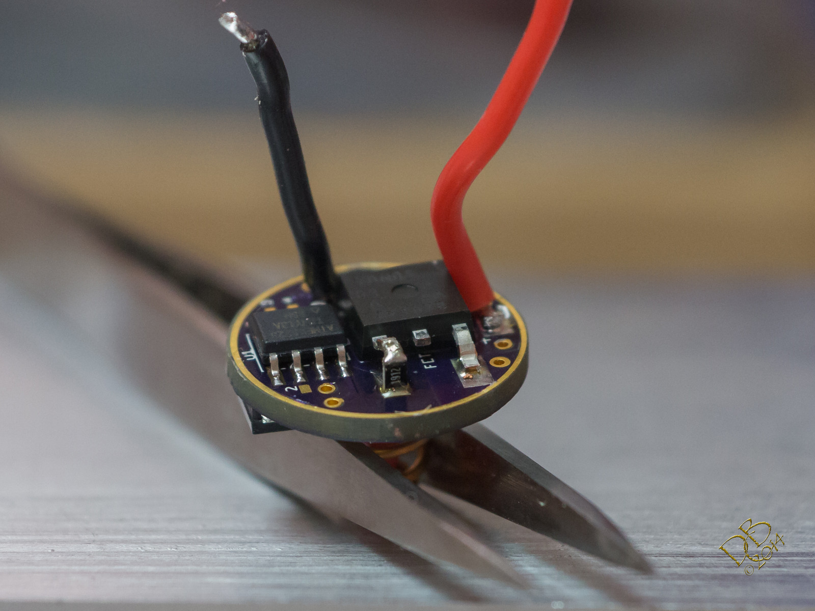
The #1 pin goes where the dot is on the board. The gate resistor you can add by simply bending the pin up and then straighten the tip, opposite of the ground leg, such that the resistor will stand up under it like a “tombstone”. Then you can scrape a slight bit of the masking off the ground pad for the pull down resistor to bridge to the gate pad.
Works quite well.
I did actually order the new boards, but doing it this way a few times isn’t a big deal.
Ok - got the dot. Pics are too dark to see orientation of MCU. I know V1.1 doesn't have R3 and R4 -- that's why I'm asking what to do. Are you saying V1.1 works perfect 100% without R3 and R4, then why were they added?
Hhhmmm. This is scary (scaru?). Is this project still in progress then? What are the 2, 3, 4 pads for? I see they connected to pin #4 (pwr)?
If the white dot is pin #1, is the pic in post #267 with the MCU in upside down? So it's totally bad, mis-leading, confusing?? Or am I confused?
Edit: Ohhh, see if was pointed out later. Nasty pic leaving in a thread like this. Again, if one thread, one post was correct and had all the latest info, this wouldn't be a problem. Maybe it's too early to finalize the info, dunno...
Soo, guess this resistor is needed, or else? What about the other resistor in the V2.0 design? Not really proven necessary/needed?
I'm assuming for now, I can scrounge other parts off an existing Nanjg? I got a couple of spare Nanjg's so not a problem for me. I got bare FET's and Tiny13A's, but not the other parts. I do have variety of resistors though (FT variety packs), so probably have a 100 ohm around, or can get one tomorrow.
I screwed up, my very first one and I put the mcu on backwards! Thank you for pointing that out again. lol
The pic above shows it right, with yet another mistake, wrong resistor.
You don’t need to use the pulldown resistor, the 10K one, works fine without it. If you’re going to use a really low moon mode then 100 ohm works best on the gate resistor (R3) If you don’t use one there you can’t use a low moon mode. Matter of fact, on this board, if you don’t use one at all the middle modes won’t work at all. So you have to use R3, and 100 works best for a lower moon.
Edit: R4 is something to do with allowing a full bleed of the PWM for the Moon and low modes to not stress the MCU? Something like that. I’m sure someone will be jumping in here shortly to tell me how wrong I am on that, as I tend to misunderstand a lot of things lately, especially my wife.
STAR 2 is in front of pin 6, should be pin 5. So if you want to engage moon mode through the STAR 2 you need to bridge pin 5 to ground, the outer ring is easiest.
Yes it works. I've built several on the BLF boards, both 1.1 and 2.0. I don't use the pulldown resistor but I do use the 100 ohm between the gate and MOSFET.
I built one yesterday or the day before. Build it just like you would the 105c as far as the Zener mod goes. Works like a charm. So you won’t even put the diode on the board, put the 200 ohm Zener mod resistor there instead.
I’ve got one in my M8, and just built another M8 for a friend.
The state of confusion is my fault. I hold my hand up for that. However, in my defense the very first driver I was asked to design was simply a reworked SRK driver. And by reworked, I mean it was copied tit-for-tat, but with a friendlier MCU was added. Now because it was basically just copied, no gate or pull down resistors were added because the original did not have any. This should have set off alarm bells for me as this is not the first time I've used FETs in a design and I understand exactly what these resistors are for. Nevertheless they were forgotten.
So why do the 15/17/20DD have the same problem? Because when I was asked to create these effectively smaller SRK drivers, I thought "piece of cake" and simply resized the boards and moved bits and pieces around. The schematic was (apart from the 15) identical and completely un-touched between all the various revisions.
Hence the problem that started on the SRK, manifested itself on all the FET drivers.
However! Why some are working and some are not is completely beyond me and makes absolutely no sense what-so-ever.
Electronics. Great when they work. Pain the arse/ass when they don't!
Mine work fine, on multiple fronts and I thank you! My favorite lights are now all performing exceptionally and it’s your fault! From the little Texas Poker to the mighty M8 and M6, and the newly modified C8 with Bucket copper pill is kicking some serious amperage booty, if not making the 2700 lumens I expected it to.
All because of your boards. I don’t know squat about electronics and have made every mistake in the “Don’t Do This Book of Horrid Electronic Wizardry”, but have managed to sort it all out with the help of some very patient folks here.
A new chapter is being written in DIY flashaholism and I’m very happy to say I’m in on it! Woohooooo!
Sorry Tom, the idea was to have projects posted in this thread with links to other threads where detailed info and discussions take place but that didn’t happen and I can only edit what goes into the op.
The need for R3 and R4 is not well understood but easy to deal with whether the board is designed for them or not so either V1 or V2 will work. R3 goes between pin 6 of the mcu and the gate and R4 goes after R3 between the gate and ground.
The how-to threads for the various versions haven't happened yet because I HAVEN'T HAD TIME YET. I'm currently more than a little overloaded doing other people's stuff!
I have the boards, and the components, and some different FETs to see if the resistor/no resistor thing is specific to the Vishay 70N02s, or just something else altogether, and BEFORE I can post a definitive how-to I need to get a handle on how it all works with which combination of parts. I'm not crazy about adding the gate resistor, since it's been reported that that lowers the low mode significantly, which can only be happening because the resistor is preventing the FET from being fully switched on at very low duty cycles, and that's something that should be avoided if possible. If it can't be avoided, then I'll just have to accept it.
There were no issues in the SRK board that got carried over to the other designs, the SRKs have been and still are working with the 70N02 and no gate/pulldown resistors, just like the 'JB' driver it was based on.
Relax, what’s done is done. It just makes it difficult to follow the discussion when the topic changes every few posts. When those threads do begin we can post the appropriate links. No biggie.

 Hhmm... did someone do this already? Hope so - should work, right?