OK. Well, I guess that means I’ll have to change it back to a single 7135 and add R1/R2 back. While I’m at it, I’ll clean it up a bit. Thanks for stepping in here and advising, DEL!
Here, let’s try this one. :innocent:
If you cut the 7135 tabs (custom footprint) and used 0603 components, you could fit it all with a little space to spare:

I’ve used a 85 with bent legs here, it’s a little bigger than your MCU footprint, but still have a little wiggle room. Visible border diameter is 12.5mm.
Also, there are 10uF 0603 caps. Here are the ones I use: http://uk.farnell.com/tdk/c1608x5r1a106k080ac/cap-mlcc-x5r-10uf-10v-0603/dp/2211164
They aren’t X7R rated, but do you really need X7R ratings for this driver?
Thanks, Mike! That looks really good! I do have 0603 components on my latest board revision. The light I’m planning to use this driver in has a 12.5mm shelf, so your design here will fit in the light. I left it at only one 7135 on my design so that all the components fit into 11mm diameter, because that could fit in a lot of AAA size lights, whereas 12.5mm seems to be less likely. But, when it comes to actually doing my mod, I might still go with the two chips instead of one. I guess I haven’t really decided yet. ![]()
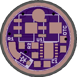
Here ya go! I had a few hours to kill at Doha international airport. You did say ATtiny13a MMU didn’t you? I don’t know what footprint you used but it looks pretty big so I downloaded one from Farnell specifically for the 13A MMU. The visible outline is 11mm in diameter:

I’m not sure what pins your using, but pin changing is pretty easy. I put the 7135s on PB0, LVP on PB2 (ADC1) and off time cap on PB3 (ADC3).
That’s awesome! Thanks again! Now I just need a source for that 10-pin MMU chip, pre-flashed with custom firmware, because I don’t have flashing hardware and don’t know how to do it anyway. :innocent:
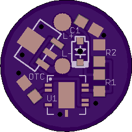
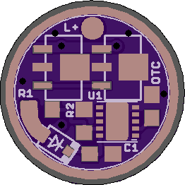
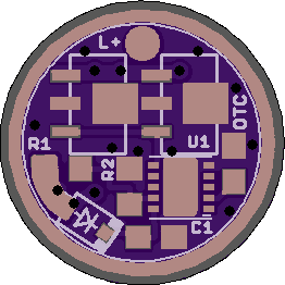
Here’s the new board, based on the layout Mike presented above. I did ask Richard about the MMU, and his website simply had the wrong picture. The chip he sells is the 10 pin chip. So, this board gets the smaller chip, leaving room for the second AMC7135 regulator, all within a 11mm outline. Thanks to everybody for the help!
Looks good! Don’t forget about the pin changes if you have made any. Make sure the firmware you are going to use is using the same pins as the driver. Forgetting will cause a heap of frustration. Update when you’ve made some.
Thanks for the reminder about pin changes. I threw this together, directly copying your design above as much as possible to avoid having to think too much. I didn’t even take the time to verify what pins are being used for what. But, I started with my own simple driver schematic in Eagle, and the air wires were connected just like the traces in your design, so I figured that was the “right” or “standard” set of pin connections for the firmware we use around here. It’s going to be important that I don’t do anything weird with my drivers until I have the ability to flash my own MCUs, or find someone willing to flash them for me.
I have one more update that I want to do with this board when I get some more time to work on it. The 12.5mm diameter driver size will work for the light I have to mod. But the ability to get all the components to fit into the 11mm outline will allow me to make one more change that will make my planned mod easier.
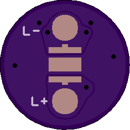
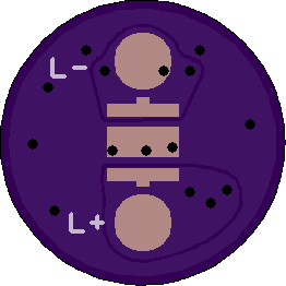
OKAY! This is a major change! I had this in mind from the beginning of this project, but I just now got it accomplished. Please let me know if you see any errors or have any questions or concerns about my design. This is the actual board I’ll be ordering for my little light, if there isn’t anything that needs to be changed between now and when I get a little money. I’ve not only used Mike C’s component layout, but also his brilliant idea of using a wire bridge across components as the positive contact for Batt+ in order to save board space. That little bit of exposed copper between R1 and the diode is the actual Batt+ contact point. The little pad marked L+ (on the driver side) is just an unconnected place to solder the other side of a wire bridge. The L+ and L- pads on the LED side of the board are for connecting to LED (s) on a separate MCPCB or some other arrangement. I’ve taken down all the earlier revision boards from OSH Park except the latest V4.0 board, which will stay in case it might be useful to somebody.
Oh yeah. I just want to go ahead and say that this will be a pain to build. It’s so tiny, so cramped. I’m going to celebrate if I get one successfully built and working in my little light! :partying_face:
Neat. I like lower brightness leds, not barn burners, and I like circuits that really use up much more battery power, leading to a longer runtime.
You’ve done a nice job of maximizing the ground plane but you need to add a lot more vias all around the ground ring and all you can fit of the smallest diameter Oshpark will do in places where more than one will fit, otherwise the largest single via that will fit(i.e., maximize through the board copper). Think of the thickness of the board as volume for more copper and upgrade from insulating plastic. Add more L- vias (= yet more copper) and L+ can add more(as many of one as the other, they both carry equal amount of current).
I know that Pilotptk did some designs along with Scaru for thin fr4 boards but with multiple vias from the led heat pad through the board to a solder able surface. Other than that I haven’t studied the mmu pin layout.
Fwiw, the 7135 specs reccomend 1000 square mm of trace area to dissipate only .7W and with a board mounted led you will have more than 3 times the heat(closer to 4x including the 7135’s) with only ~220-230 square mm trace area. You will need all the copper and solder filled vias you can fit.
Thanks. I’ll have to take a look at maximizing the vias and traces, I suppose. I just thought that since it was small and low power it didn’t need as much attention. I guess I was wrong! ![]()
Feeding a separate mcpcb it would be fine. Low power is relative though. 5A on copper DTP vs 3A on aluminum mcpcb with dielectric vs 750 mA on a plastic insulator with a few milligrams of copper traces, it’s all relative.
Well, relative is exactly what I was thinking, but in a different direction. The planned emitter for my light is a XP-E2 R3. This emitter is rated to handle up to 1A current. (If that won’t work, I also have a XP-G3 lying around! ![]() ) As has been discussed previously on BLF, CREE’s ratings seem to be good for emitters mounted on a cheap aluminum mcpcb with dielectric, and even in that case, their ratings are probably conservative. My thought is that the emitter itself can take some amount of heat soak without damage. In this case, since the driver is on the same board, I’m assuming that the components can do the same. The longest distance from any point to the nearest edge of the aluminum host is about 6mm. That’s not very far. I’m planning to order the thinner boards with 2oz copper from OSH Park, so there will be less insulating material and more copper already. I plan to add more vias where possible and maybe widen some of the power carrying traces, as you suggested. I’m hoping that will be enough.
) As has been discussed previously on BLF, CREE’s ratings seem to be good for emitters mounted on a cheap aluminum mcpcb with dielectric, and even in that case, their ratings are probably conservative. My thought is that the emitter itself can take some amount of heat soak without damage. In this case, since the driver is on the same board, I’m assuming that the components can do the same. The longest distance from any point to the nearest edge of the aluminum host is about 6mm. That’s not very far. I’m planning to order the thinner boards with 2oz copper from OSH Park, so there will be less insulating material and more copper already. I plan to add more vias where possible and maybe widen some of the power carrying traces, as you suggested. I’m hoping that will be enough.
I had said long ago in another thread that most of the LED testing around here seemed to be how far they could be pushed with ample thermal conductivity and that I was interested in testing how far I could go with a minimum thermal path. I’m still working on that idea, although my testing isn’t done with charts and graphs like others use. I’m just building things and seeing what happens. As a last resort, if need be, a “turbo” timer can be added to the firmware for this driver. But, I still think about some of the more extreme builds I’ve seen around here. Remember Dale getting his little Texas Poker to put out over 1000 lumens?! That tiny light, made from Titanium, pushing the limits of what a 10440 can do to a XM-L2, is one of the many inspirations for this project. My light is made of Aluminum and will be much lower powered, so I think I have some (relative) wiggle room. ![]()
Does this picture show up? This is a render of my board with proposed locations for new vias showing up in red. I added 5 new ground vias, for a total of 9, 1 new L- via to bring it up to 3 total, and 2 new L+ vias to bring that also up to 3 total. I haven’t worked on trace width yet. I don’t have access to my computer with Eagle right now, so I’m playing around with MSPaint. ![]()

Here is the board with added vias.
I reference charts and graphs quite a bit but I’m still more of a seatofthepants type myself. I just figure in a case like this if there’s room for more vias it can only help. In particular I was thinking of the LD-1, 2, 3 which have the ground ring peppered. In your case not for current path but for heat path which is on the other side of the board and also allows those particular vias to be solder filled.