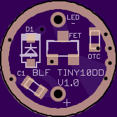
Redux of the boards, relocated the C1 in order to have stable mode changes, no longer need the load resistors on the gate (less components means they cost less)
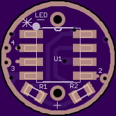
BLF10DD
Top
Bottom
BLF12DD is the exact same as the 10DD just with a 12mm diameter
I don’t have the files in dropbox yet…will have them there shortly
OK…Mattaus was kind enough to give me his brd and sch of the 7135, I have tweaked them to now be compatible with the IRLML2052, pads and all (so no need to cut the 7135 traces
Only change from 10DD to 12DD was a larger ground ring, and I moved the resistors ever so slightly on 12 to loosen things up a bit, added R3 to be a buffer between the MCU and the gate of the FET
Per request I will be modifying with a pad for a 100-130Ω resistor for shock isolation between the FET Gate and the ATtiny’s PWM pin #6, expect a revision soon
On the Tiny12 I might also go in and thin out the bottom ground ring to give a bit more space
Especially when mounting on a contact board, I add the leads last so I wouldn’t even see it if it happened.
This isn’t really OSHPark specific but what are a few good hosts for the 12mm driversedit never mind it doesn’t have a center contact so it’s not really a direct fit/replacement. I see now.
Another thing I notice- stars 3 & 4 arnt start at all but ground points to go direct to the MCU leg, I’d much rather they were real stars that ground to the ring. Probably have to move #2 over some tho and have a trace go to the pin, that one might not be possible, dunno.
Actually it’s a jumper point from the MCU’s pad to a ground pad, no real way to make a star, just have to jumper that gap and it’s the same as grounding a star
Oh not worried it’s not star shaped but see on the 15DD V3 the closer set of pads to the leg are actual contact points connected to the leg and they jumper to other GND points. In these smaller ones you wouldn’t need the extra GND pads cause its close enough to the ring to make the connection directly.
IDK, its not necessary, it works fine as is, just an idea.
I’ll see what I can do…plus it could use a few more teeny via’s anyway, the more path it has the more current it can handle without stressing the traces
CK- in my preliminary tests I found that above ~1.5A mode switching was erratic without R3 but stable when I added it. T his was with standard Qlite firmware meant for 8 × 7135 drivers. The same thing occurred when I tested that funny FET led4power is using on his driver. Until we know the cause it would be a good idea to allow space for R3.
I always recommend having led +/- opposite each other since that’s the way mcpcb’s are laid out and matching the two allows for minimum space consumption.
Making the ground ring just a tad smaller(but not skinny) will give a bit more room between R1/R2 and pins 4&5.
If you were to design a Zener mod for this board the resistors don’t need reverse polarity protection so R1 could pull straight from L+( the resistor values are different for this mod) eliminating one of the traces under U1. I’d also reverse R1/R2 for this.
The led+/- pads were originally designed this way on the Tiny 10 so that the board could be oriented with either side facing the led with the idea that where possible the “star” pads could still be accessed.
BOTTOM
Moved some stuff, shrank the ground ring a little, cleaned up a bit, added the 100-130Ω (R3) solder pads
Honestly this is about all that can be done…there isn’t a whole lot of room
The ground rings yes (reduced in diameter), and the via’s I made them all .3302 (and removed the stop layer on the ones that weren’t being used as ground positions for the stars, do they need to be bigger in diameter?
I don’t know. I seem to remember someone saying make the vias bigger on one of the other boards (Helios, maybe?) but I’m not sure which board or who said it. If these are the same size as on the 15DD and 17DD then it’s fine. I’m guessing too small reduces the current capacity. .3302mm sounds large enough though.
Not sure who said it but someone said multiple smaller ones can carry more current than one big one…I think it was wight
I ran the signalling traces a bit thinner and made the power traces alot thicker…not much current flow in the signal trace, but can be ALOT of amps in the power traces