I've done it, not on these of course but on one built similar. It's thicker than you'd think.

I've done it, not on these of course but on one built similar. It's thicker than you'd think.
did it work out? (even with the indentation?)
Well, sure... took a disturbingly large blob of solder paste, but it physically attached like normal and light came out the correct end when put back together.
I’m going to point out that solder has lower thermal conductivity then copper or aluminum, so the thicker layer you use of it, the less advantage over standard stars you will have (i know of no one who has tested exactly how much less though), though i think it will still be somewhat better then the standard star
Comfychair, where did you get the copper base from?
Anyone has tried the DX copper base one? I wanted to buy those before and scrap off the di-electric, but to be honest the DX picture doesn’t look like copper at all to me.
What did you use for scraping? It’s quite a small area to work with.
I wonder if the alu base one can use the same trick.
not like that: you can not solder onto aluminium
I used a razor blade to cut along the edges, then a tungsten scribe (tig weld electrode, kept sharp enough to draw blood if you just look at it funny) to scrape/peel away the middle. Some of the really tiny Dremel engraving bits would work as well.
Well, solder has a thermal conductivity of about 60 W/mK. Copper is about 385 W/mK. Dielectric is somewhere between 0.5 and 3 W/mK. Thermal glue is usually < 3 W/mK.
So these pads without center layer, a lot of solder and a good metal to metal contact will still be better than Fujik'd Sinkpads. :)
If all the parts in that thermal path were the same surface area, then those numbers would be telling the whole story. But they're not. XML thermal pad is 13.3mm2, 16mm MCPCB is 201mm2 not counting the wire notches. Massive difference in area. So a relatively poor thermal conductor can still be adequate if its area is large enough.
My original question had to do with cut-pad performance vs a Sinkpad performance…
I’ve never reflowed an emitter, and I’m guessing the answer is ‘no’, but out of curiosity… would it be possible to use a XP-G led on a cut-out XM-L FT copper pad, so good contact and little solder can be used, with +/-’ves bridged to the contacts? (I’m guessing they don’t reach because of size difference)…
I’m guessing you’d have to be pretty desperate to want to do this… more curious than anything… ![]()
Uh... no. Wildly, crazily different sizes. Neither will fit on the others board without either shorting or not making contact.

Just a thought, if you want you could also scrape of the dialectric layer then use a suitable sized punch to gently raise the centre pad, then reflow. Pretty much like a sinkpad. With a bit of fiddling and checking it shouldn’t be too hard.
You cant attach the emitter to the PCB without solder. So you have a solder layer of lets say 0.05mm for Sinkpads and 0.15mm for copper PCB with removed dielectric.
Measurable of course, but pretty much irrelevant in real life application. LED-tech copper PCBs dont have a raised center and those perform as good as Sinkpads when it comes to massively overdriving emitters.
For me its still the application that matters.
Maybe someone who has a good temp sensor can run test for us?
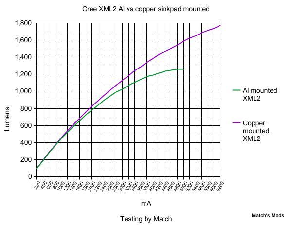
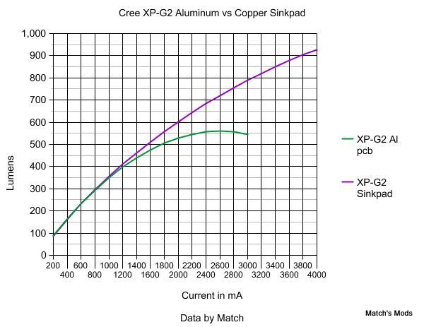
Comparing Copper Sinkpads, Alu Sinkspads, Copper MCPCBs, and Alu MCPCBs.
Hehe… OK definitely not… thanks for the comparison!
I’m ignoring the the thermal glue, because you can choose to use it or not use it on a regular pad or a sinkpad, so its an eliminatable variable.
You would have to do some testing or a thermal analysis to be able to say for sure, the dielectric layer is thinner then your solder layer on that setup, so even though solder has superior conductivity, at some point (and i have no idea as to where that would be) the thickness of the solder would reduce output to where it would have been originally with the dielectric. This could happen at 3mm or maybe 2 inches thick, i have no idea where that point would be.
That said i don’t have data, only an opinion from chatting with a respected member who has done lumen testing who says he has subjectively noticed a lumen decrease when he reflowed an emitter onto a sinkpad type surface and the solder layer came out thicker then he was hoping.
I highly doubt a visual difference in solder layer thickness, as some recent threads showed, some people can barely make out the difference between XML U3 and XML2 U2 side by side. Also, in this case solder would replace the dielectric.. not add 5mm of solder between star and LED.
But hey, placebos only work because you believe it. ;)
Light meters don’t lie though ![]()
At least not when doing comparison before and after… Same amps, same emitter…
A *good *copper MCPCB can do wonders… Everything that works against the thermal transfer will get you closer to an aluminium MCPCB.