How shapely can the pads be then? I guess this means another do over, whoopee. :Sp
You can adjust the roundness of the corners. 100% will create a circle if the pad is / was square.
This is an image of the tstop layer.
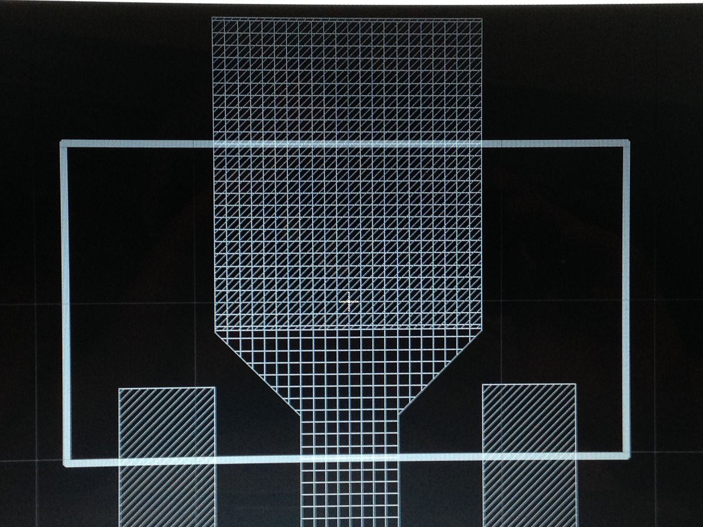
Overlaying the polygon which encompasses the entire ground pad is a rectangular SMD pad. On the brd. The route command connected the rectangular gnd pads ignoring the center pin but if the copper pour is continuous and the stop occurs where it’s shown in the larger polygon then what’s the difference between this and a “real” arbitrarily shaped pad?
Found the drc mask bits, thanks. How does one tent one side of a via? Like the heat sink vias under the buck ic on the knucklehead driver, they are unmasked under the ic but tented on the backside.
Hmm, check that the polygon is set to solid. Just created this full gnd pad.

Simply tent everything. Use the stop layers on your BRD to unmask whatever you want (place a filled circle or whatever shape is appropriate). At first I thought I might have a lot of need to do that, but I found that I almost never needed to do it. EDIT: There’s rarely a need to do that because typically the side I want to be bare copper is already sitting under a pad or something that’s already bare.
As wight said, If a component already has tStop then a via you place within there will be exposed copper due to the component tStop. If you also want the back of the via to have bStop then right click it & check stop.
Thanks guys, I’ve got the vias sorted. Air wires are a pita. After connecting up the board you still find these odd bits like lint scattered hither and yon and drc doesn’t like it when you go back over an existing trace like a kid with a crayon. Anyway, here is the latest version.
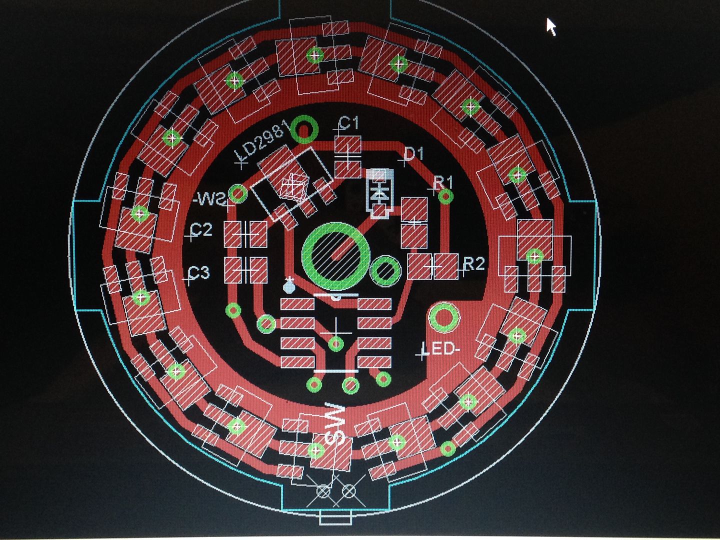
I’ve added an SMD edge switch that I ordered off eBay. They posted the data sheet with measurements and land pattern. The board isn’t very crowded but 15 chips should be good for ~5.7A and having the switch mounted to the board means room for a larger sink. I may look into shifting the control circuit to the battery side and add more chips or make an FET version. This one is set up to use either standard 105C firmware w/stars or off time cap (C3)or e-switch firmware even though I haven’t the faintest idea about any of it.
For a first up you have done an exceptional job RBD. I'm glad I stayed out of it. 
What’s up with the two drill hits under the button?
Airwires should never be a problem if you pay attention when ROUTEing a trace. Make sure you hear the “boop” when you complete the ROUTE of the segment. If you don’t hear it, your trace did not end where it needs to. It might be close, but this ain’t horeshoes and hand grenades.
Also, you can get those yellow “X”’s if you ROUTE to a via…
Just found out you can do the same thing and save your layer settings, you can make one setting for “top”, one for “bottom” and one for “working” or whatever you want. Again you get it set how you want it then right click and go to new, then enter “alias for current layer selection”.
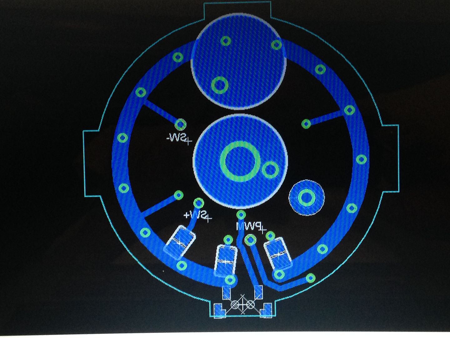
Recommendation, there are some very close traces to the ground pads on your 7135’s, they are signal traces and can be thinner and/or moved outwards to allow for more clearance (or to dress it up…make an almost complete circle)
Either way that is an AWESOME design man!!
Wight- the switch has plastic locator pins to take the shears strain of button presses from the the solder pads.
Mark- I’ll keep trying. The first attempt showed a lot more drc errors than this one but I still have a ways to go.
Brian- thanks, how narrow(in mm) can the signal traces be?
I’ve got mine setup for keyboard shortcuts. It saves a huge amount of time.
The signal traces can be very small. OSH Park guarantees the integrity of traces as small as 6mil. I took a glance at two functioning designs just now: Mattaus’s Knucklehead v3 and my 22mm 7135 v016. Mattaus used 16mil on the Knucklehead. I used 10mil on the 22mm 7135 v016, for the MCU Vcc trace. As you can imagine, the Vcc trace requires significantly more than a signal trace. In other words I don’t see a problem with going as low as 6mil for signal traces when needed.
How do you setup keyboard shortcuts for the layers?
I use the shortcuts dialog and use the “DISPLAY” command. Take a look at the Eagle help file under “Editor Commands” for the details on how to use DISPLAY. It’s pretty flexible. I just set it to turn on and off a few key layers and leave everything else alone - when I want to mess with them I go into the layers dialog and do it.
1mil or .254mm (thicker they are the better, but in case, you can make them the minimum thickness…it’s passing signal, not power.
No, they need to be at least .006” wide… the thinnest that OSHPARK can make. Board costs go up exponentially below that. Make all your traces as wide as possible and separated by as much as possible. Your boards will be more relaible. I always try to use 12 mil minimum trace widths and spaces.
1 mil = .0254 mm so 6 mil = 1.524 mm. My thinnest trace is .3 mm or 11.8 mil.