Hmm, well I learned something there. I’ve wasted a ton of time switching back and forth.
At first I didn’t understand, but between what you and WarHawk-AVG have been saying —— you guys were previously using the “wire” command/tool to draw traces instead of the “route” command/tool?
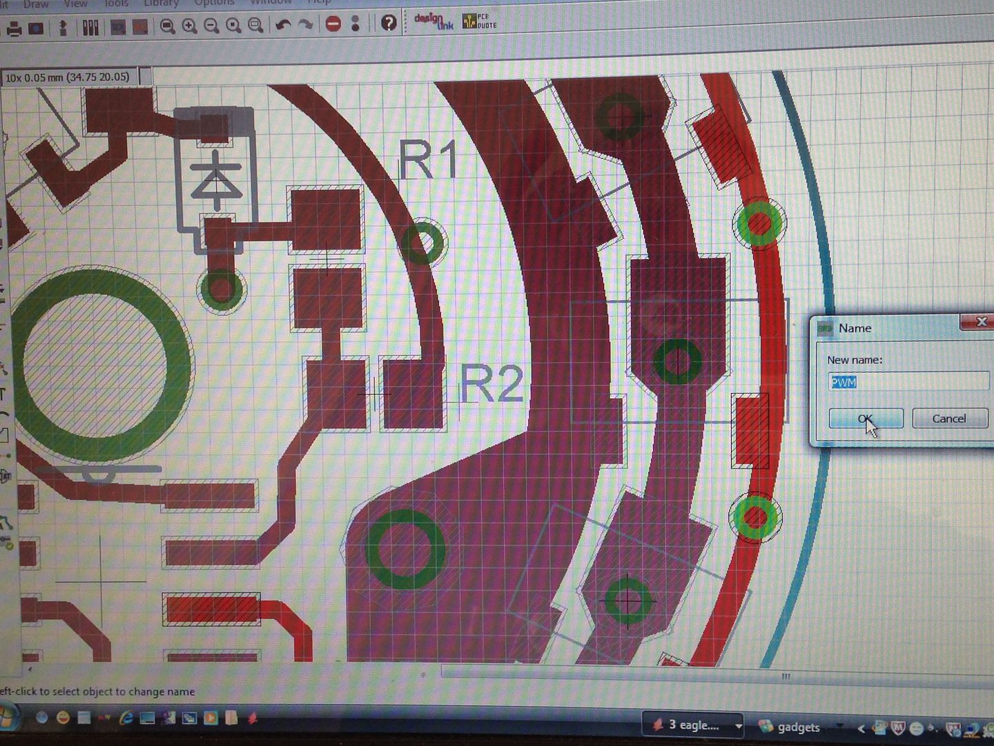
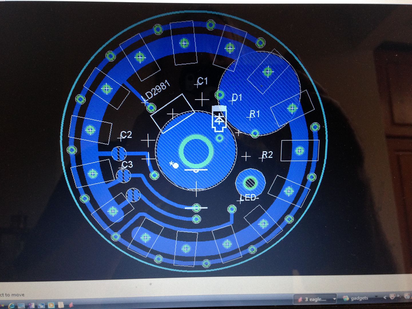
Using wire command, yes. So I should draw traces with route instead? At least now when I click the pwm trace using the name command the entire trace including pads and vias is highlighted.
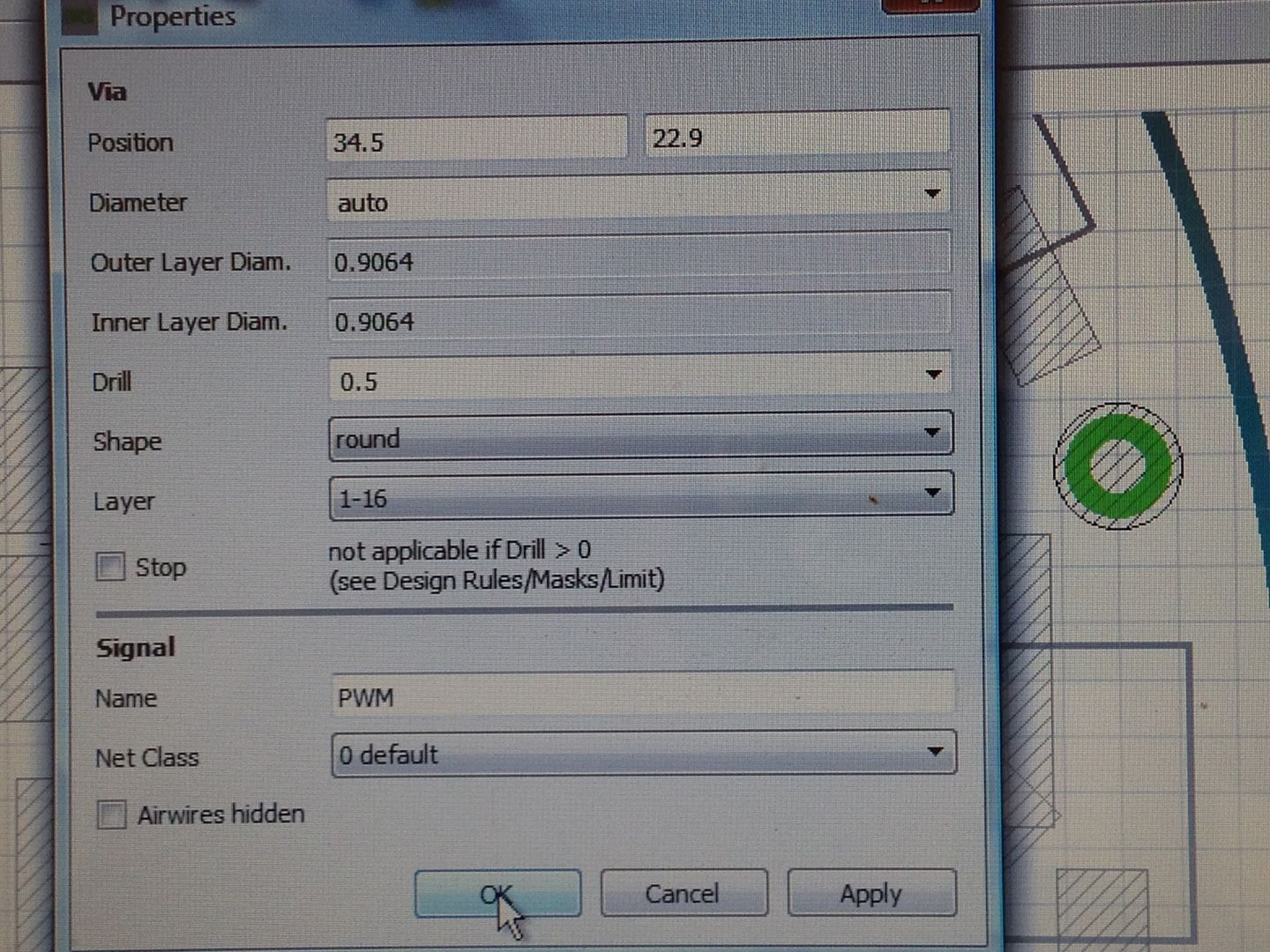
The “stop” check box in properties doesn’t seem to have any effect on the t or b stop layers for vias.
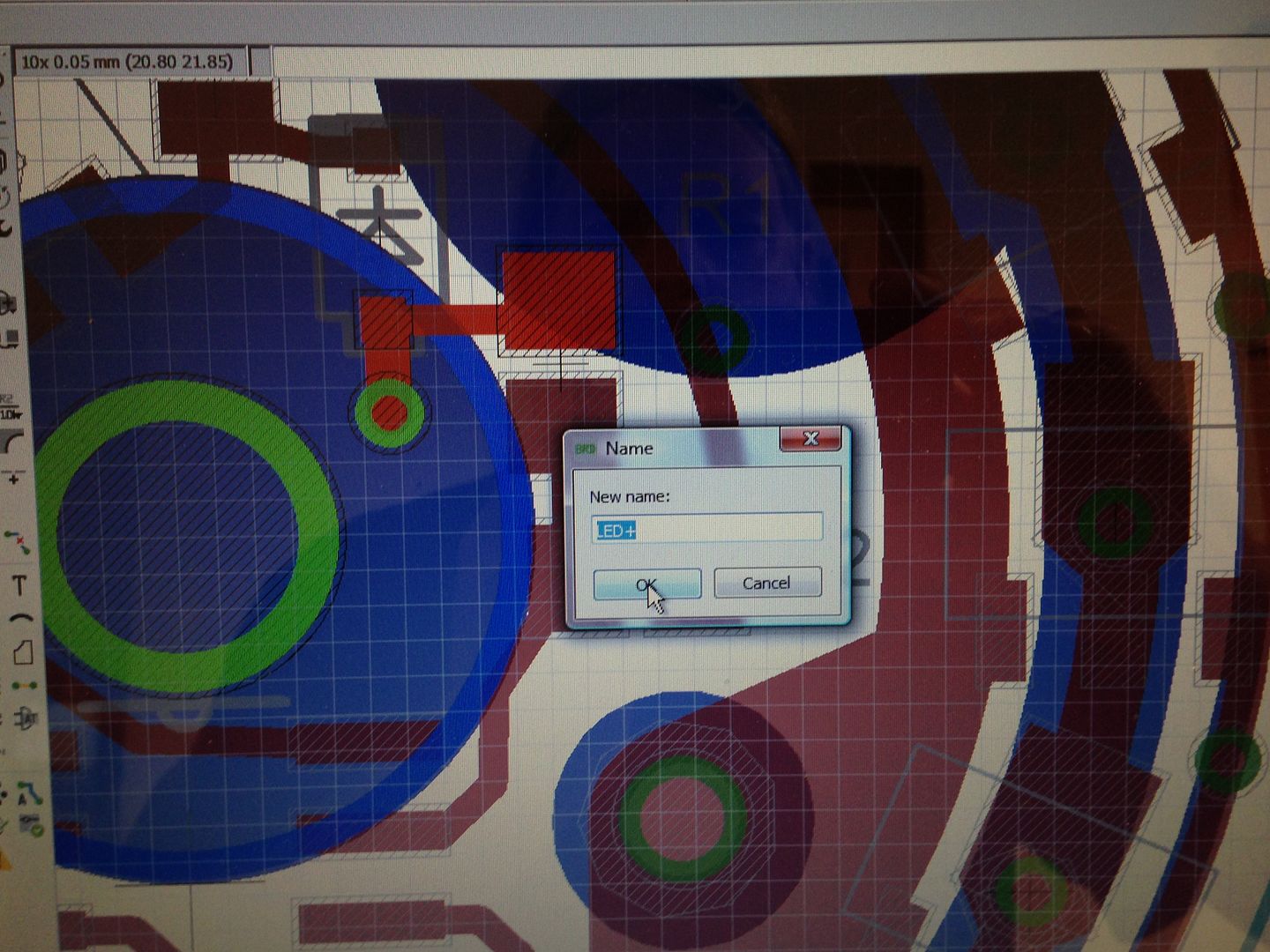
Does it matter that the entire pad doesn’t highlight here. I used the circle set to 0 to make the pad and arc to make the circle and named it led+.
How do you make the locator tabs like on the SRK boards? Would you draw the tabs first then use the arc command to connect them?
I do not lay down any copper using the wire command. I only use the route command. If something won’t connect it’s typically because I’ve made an error on the schematic.
AFAIK what Halo… said in post #93 is incorrect. That checkbox is only for adding to the stop layer (which is a negative layer, so putting things in the stop layer means stop will not be applied - in other words the copper will be bare wherever there are marks on the stop layer). You must follow Cereal_killer’s instructions in post #92 or Warhawk-AVG’s instructions in #96. (Both instructions are for the exact same task.)
EDIT: I mean to address the circles as well: I do not use any circles in the copper layer. Circles are just problems in Eagle. They cannot be attached to a Net (eg they can’t be named) so they will interfere with polygons and they won’t complete circuits. You can’t connect to them at all.
I use the route command to connect all the air wires first. Then I use whatever tools are available to make the copper pour look nice, whether that be the circle, arc, poly, or wire tool.
Form and function are equally important to me.
I hate having unconnected air wires left on a board. It feels unfinished and not 'right'. An no, hiding them does not help :)
I watched then videos and read tutorials umpteen times but it isn’t until I actually do it that it starts to stick. Thanks guys. I Like the component layout as is so how best to correct this? If I try to delete a wire that is now part of a net I get an error must do this in schematic box. Do I need to smash first, or something else? Starting over with just the air wires is an option if I can find a saved version that old. Where do I look for that?
Almost! Smash is a different thing. Instead use the Ripup tool. I think you’ll find that double-clicking with that tool will remove a lot very quickly.
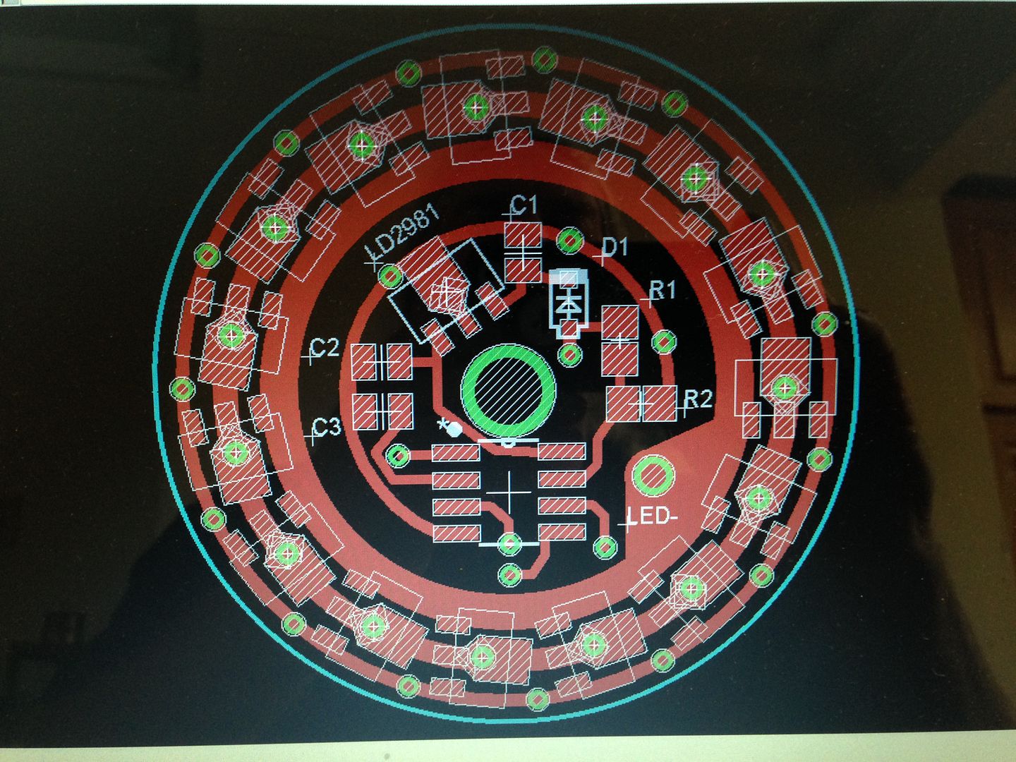
I made the ground pads on both sot-89 chips by connecting the schematic gnd pin to 4 smd pads that make up the odd shape. You can see this most easily in the tstop layer. It seems to result in extra air wires to each of those individual smd pads in each package. For the most part, the air wires can be dealt with by going over each one with the route command but sometimes a yellow X is placed. Once, a layer change dropped a via to eliminate the air wire without leaving the X but this does not work in every case and seems like pounding a square peg in a round hole.
But that's what the X is telling you - that it thinks there should be a via there. You either have to put a via there so that it can join the top and bottom layer, or connect the top or bottom trace to a suitable point on the same side as the trace. It's putting the X there because it thinks that is the most appropriate place for a via. You need to tell it otherwise.
No, it’s putting the X there just to annoy you. You need to slap the snot out of whoever is responsible for some of the things Eagle does. J)
And don’t get me started on it not letting you start/add to a route on a net except where it thinks you should… I want to route a trace on the net… OK, there is a place on the net… let me f’ing connect to it there… not at some place a mile away on the board… BASTARDS!
lol...I feel your frustration. Trust me. Sometimes I end up with a spaghetti looking trace just to get the X to disappear and then have to spend too long cleaning that up. The key for me however is not to be dodgy and just hide the layer like some people do *cough*.
Actually, I don’t get too many yellow “X”s. I use Eagle properly. Use the freakin’ ROUTE command to add etches to your board. Not the LINE command. Only things drawn with the ROUTE command are linked to the schematic. Anything you do with the LINE command on the routing layers is asking for trouble.
ROUTE you signals properly. Track down a get fix unrouted airwires.
Use the freakin’ Design Rule Checker (annoying as it can be). Understand why it is bitching at you.
Slap the snot out of the Eagle people until that add a decent way to ROUTE arcs, etc. Heck, slap the snot out of them for just doing some really annoying things.
I only use the route command to connect schematic lines/airwires. I use the line/arc/etc tools to pretty it up once it's all done :) I very rarely get problem X's. Maybe one in every 5 or 6 designs.
“And don’t get me started on it not letting you start/add to a route on a net except where it thinks you should… I want to route a trace on the net… OK, there is a place on the net… let me f’ing connect to it there… not at some place a mile away on the board… BASTARDS!”
Thanks TP, it’s refreshing to hear that when had to start on the air wire and draw over existing copper to get it to go where I wanted.
In both cases the remaining X’s are right next to a via that is already connected (and named) to the same signal on both sides. There are these short sections of air wires that cause this. I ripped up the entire board and started over in the schematic layer with just the components, and redrew the traces with the route command. A few times I could get the X to go away without dropping a duplicate via, sometimes the via appeared, and sometimes I added a via but the X stayed put. I’m about ready to print this up and paste it to a dart board next to my least favorite politicians. Each time I repeat this process it gets easier so I’m not overly concerned as long as I learn something new each time.
When making up a component in the library window I notice there are only 2 layers. Is the stop layer automatically added? I’m wondering if there is a way to draw the ground pad as one continuous pour rather than stitching together several cookie cutter pads.
To create the appropriate stop shapes you need to be editing the “Package”. I’ve just checked a random Package and the tStop layer is present and populated with shapes. On creating the GND pad in your Package: I’d use whatever combination of rectangles and polygons gets the job done.
I mapped the corners of the 7135 ground pin and tab pad and redrew it using the polygon tool set to top then again a bit larger set to tstop. The top poly filled but won’t let me name it and although the tstop poly shows as tstop in properties it’s drawn with a 90 degree hatch instead of diagonal. I plunked a large SMD pad in the pour and named that. I’ll see how that works. Don’t know about the tstop though.