Looking for Feedback on Driver for SFY55

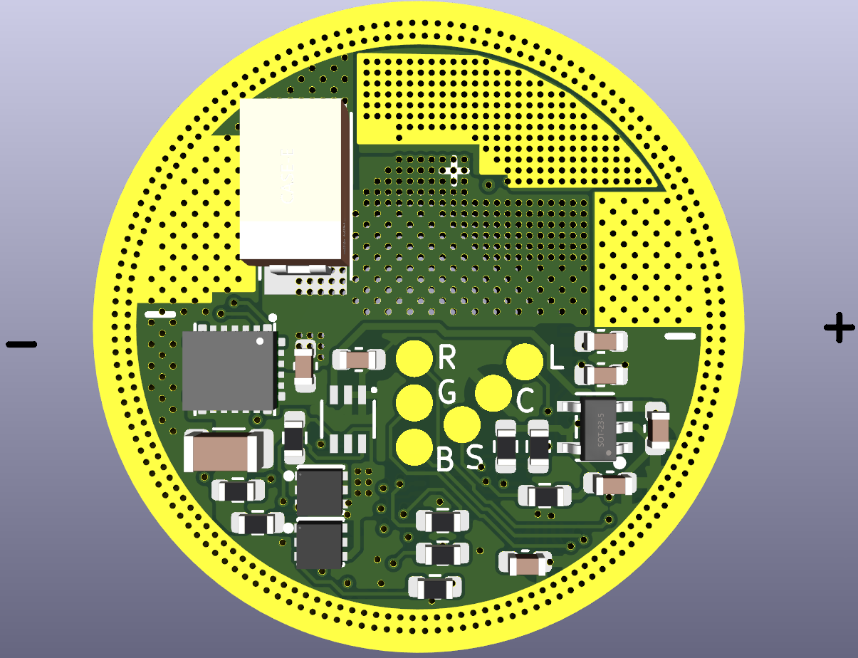
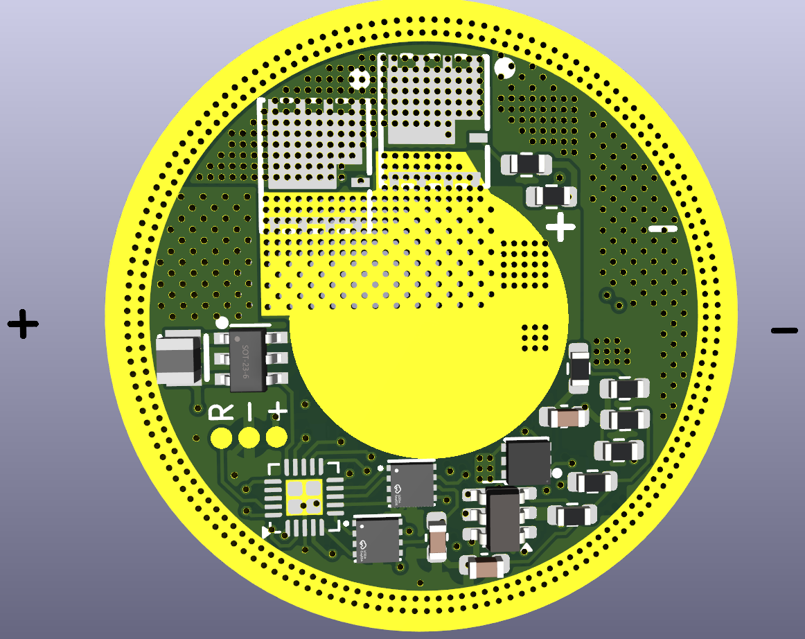
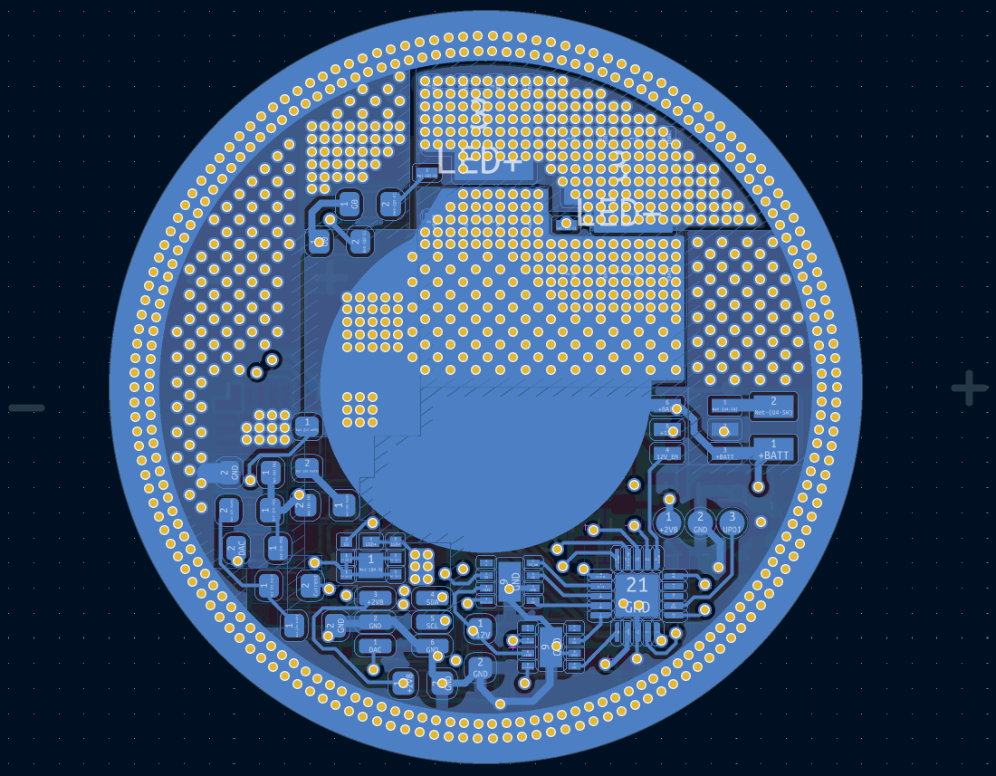
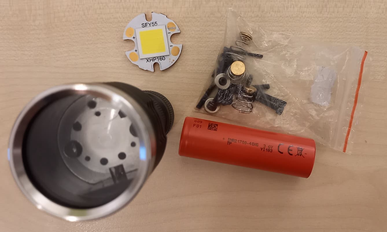
This is a very slow follow-up to my previous post. I have finally setteled on a DM11 as the host.
This is mostly due to the small size and the space for a large copper block as a heat sink.

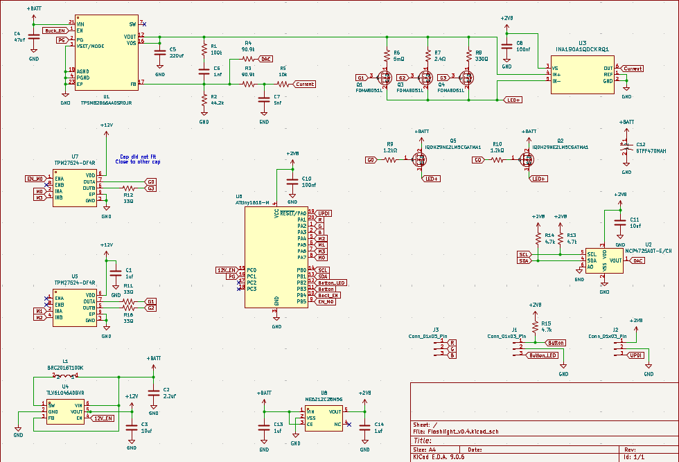
The driver is basically supposed to short an SFY55 to a tenpower 40xg for 10s,
and hopefully not burn up in the process. I also changed the dual 7135 to a 6A buck with triple shunts.
This should allow for constant current from basically invisible to 2k lumens.

The external DAC is there for finner controll of the current. This is due to the feedback network I am using
needing small steps around 2.5 V instead of small steps near 0 V like others.
But unlike others, it does not have a voltage divider tied to the Vout of the buck.
This makes it independent of the vf curve of the LED. This should theoretically also improve the dynamic range.
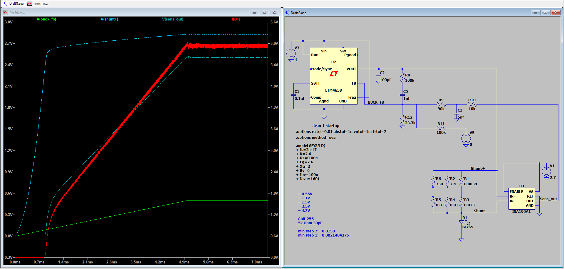
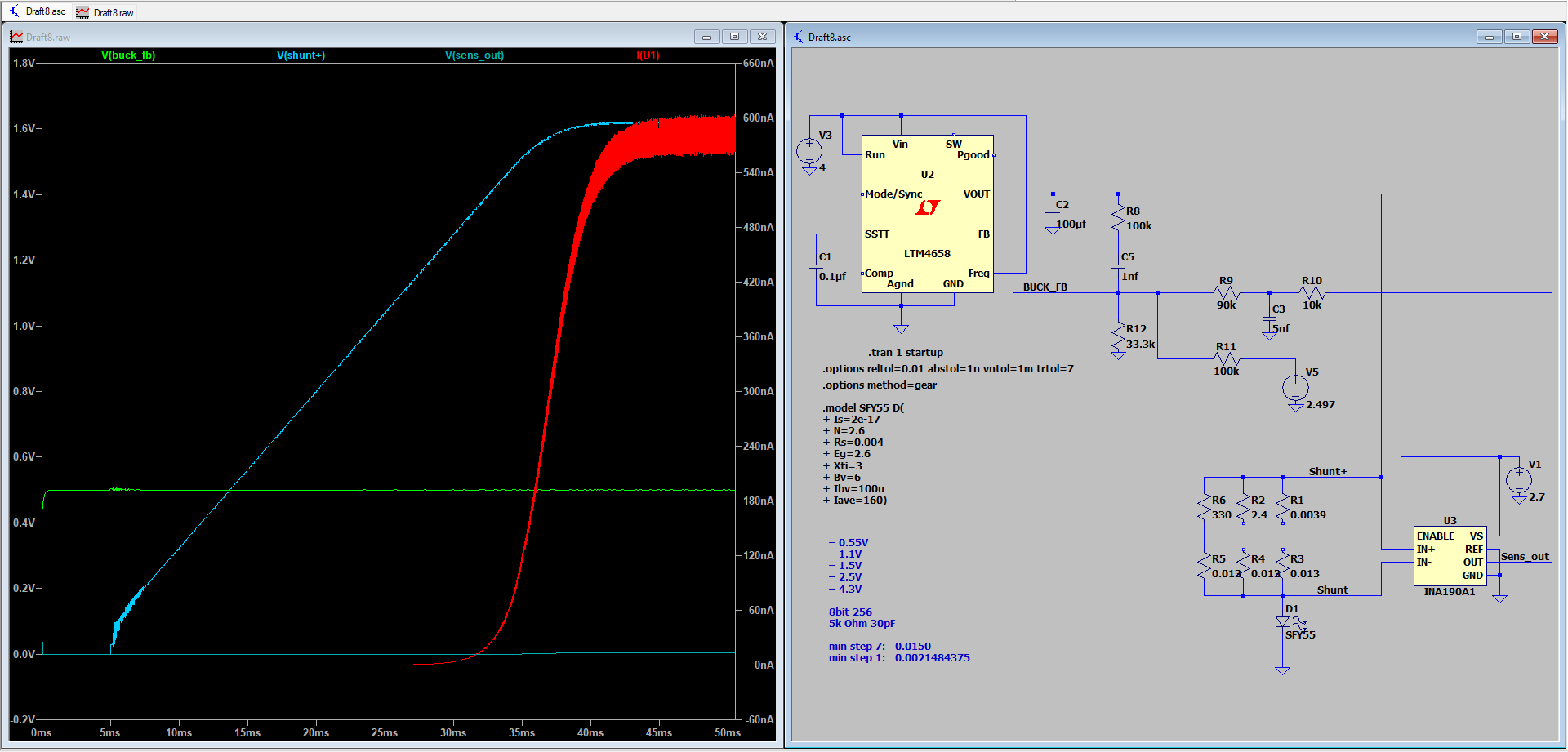
But I am not expecting to actually hit the 600 nA of the sim due to real-world problems.
It should be decent anyway, unless I made the current overlap between the shunts too small.

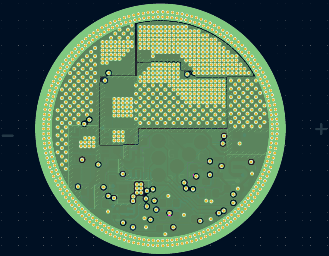
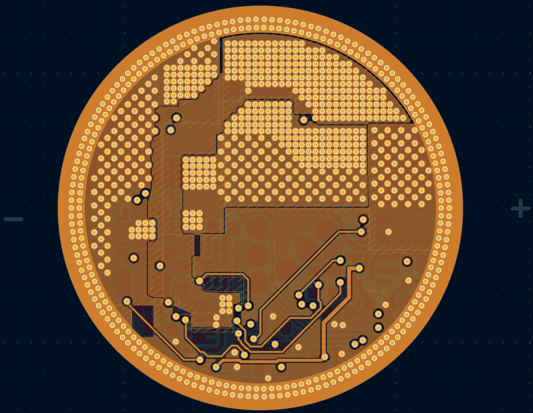
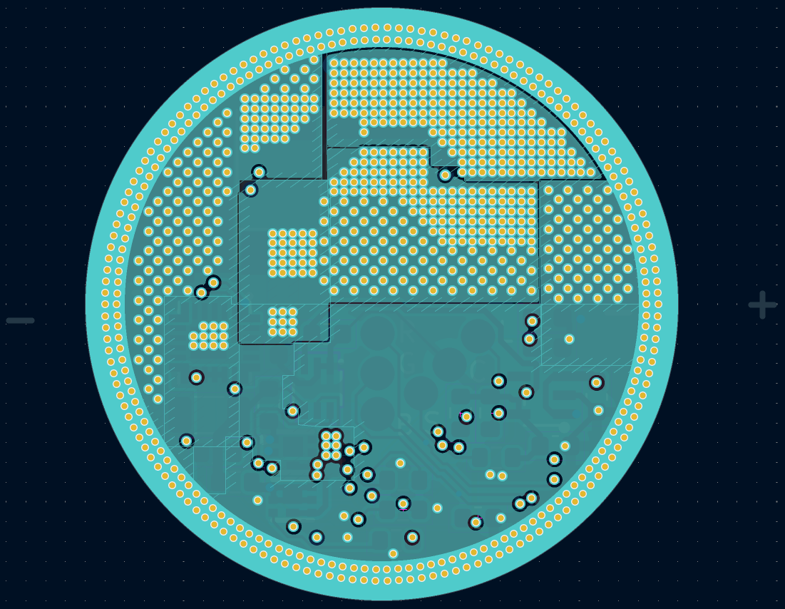
The buck in the sim is a different one than the one on the board due to me being too dumb to use PSpice.
The large cap and gate resistors are there to try and not kill my board at turnoff of the FETs.
In my calculations the inductive spike should have killed some stuff without that.

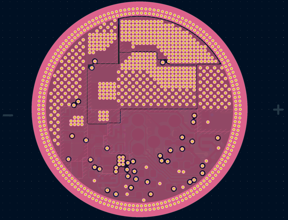
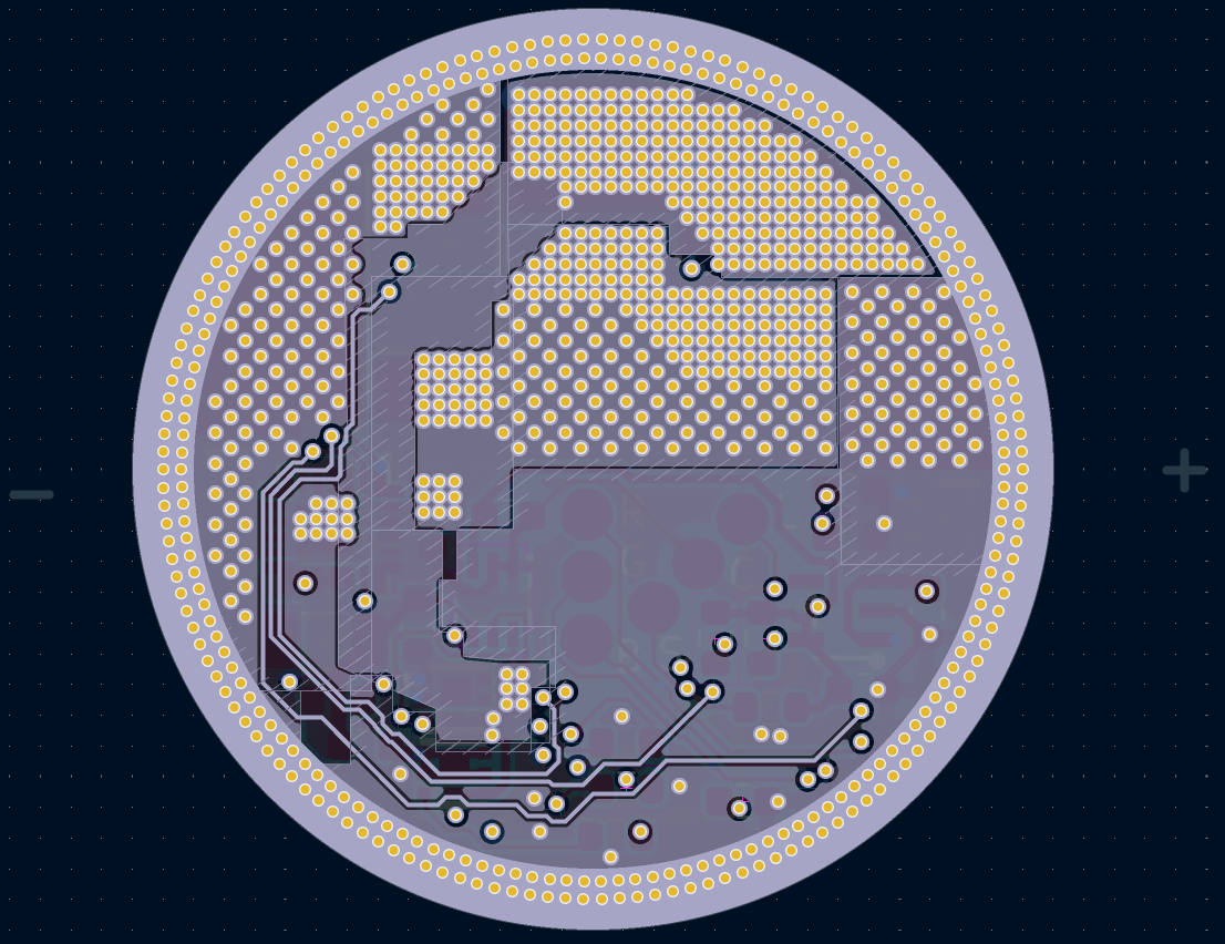
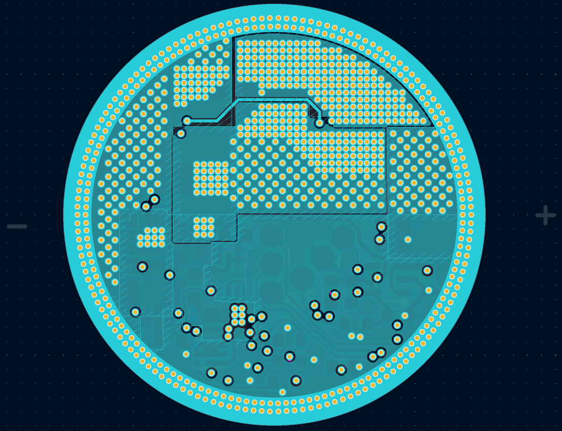
There are pads for aux lights on the board, but I will likely not use them in the DM11.

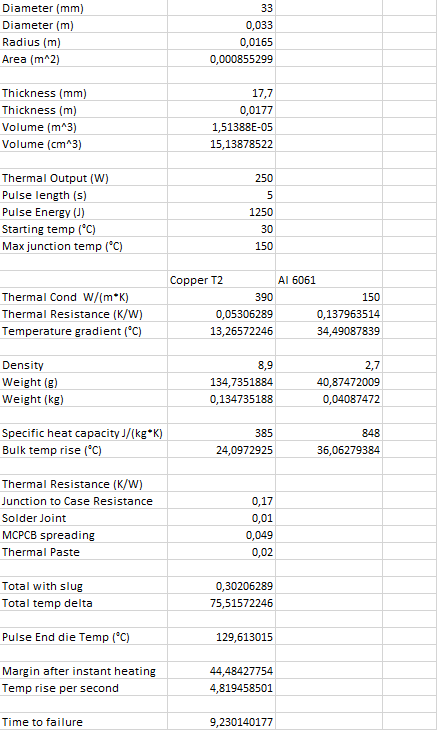
The calculation for the thermals is quite pessimistic due to not accounting for the energy needed to heat up the
-MCPCB
-housing of the flashlight
-gradient of the copper block

So while the time estimate of that is 9.2 s, I think it should survive 10 s just fine.

Of course bypass wires are being used. Currently looking at dual 16 AWG.

If someone with experience in driver design can give suggestions, it would be highly appreciated.


1 Thank

I could be wrong, but I’m pretty sure you can’t use IQDH29NE2LM5CGATMA1 on the + side like you are.
They are N Channel not P Channel.

Also where is the 12v coming from on a DM11?

2 Thanks

The 12V is from a boost converter that is only active when the FETs are being used so that idle power draw is low.
(TLV61046ADBVR in the bottom left is the boost converter)

I think I can get away with using N-FETs because of the 12V.
N-channel FETs need a certain GS voltage, which would normally not be there because you got max Vbatt to GND.
But here it is 12 V minus Vbatt to GND, which is around 8 V; this is more than enough for the FETs.
You could get their resistance even lower if you used a proper high-side FET driver with a charge pump, but I did not want to do that.
Or by making the boost converter output 15+V.

You could also put the FETs on the low side of the LED, but then you can’t use a standard buck as far as I know.
An inverted buck would be needed in that case, and they are not as common.

The arrangement I chose was the best way I know of combining a buck and a FET.

1 Thank

That’s a lot of vias… maybe too much, there’s something about too many vias close together increasing parasitic inductance, I don’t really know how significant that is but anyway you could do with fewer larger ones. Also are you using filled vias? because there are a lot of vias in pads.

The Rdson of Q1 is pretty high if it’s FDMA8051L (difficult to read), and it’ll vary between parts, drive voltage (as Vf changes) and temperature, because it’s a large part of total Rsense (about 2/3) it’ll make the current quite inaccurate. I would use a significantly lower Rdson mosfet for the high mode Rsense, it would make the current more accurate and also decrease losses with a lower total, probably a 3333 package since space isn’t an issue, personally I try to keep it at least below 1/3 of total Rsense, lower is better.

Why the 1.2k R9 and R10 gate resistors ? it’ll cripple the drive current and if you’re PMW dimming with the FETs they’ll dissipate a dangerous amont of heat because they wont be able to turn on fully (and lower current to the LED).
I wonder if it’s possible to keep the buck ON when PWM dimming with the FET to have a smooth transition between buck regulated and FET direct drive with a high side shunt(s) like this.

About the CC regulation circuit, what are R1 and C6 for ? something stability related ?

1 Thank

Yes the vias are filled and due to the current and the current per via this should be in the region of the number of vias required.
With the 18um plating thickness the current capacity per via is pretty much exactly 1A according to Saturn PCB.
I have no idea about the paracitic inductuance, but due to the low frequency its probably not a issue.
Also according to this: How Do Pads and Vias Impact Total Capacitor Parasitic Inductance?
“inductance increases with via diameter and increases with via length” (Saturn PCB says the exact opposite so I have no idea)

With the many vias I am more concerned with them decreasing the current capacity in the XY direction, but due to the copper on the other layers that gets connected though them I think its worth it.

Yeah the FDMA8051L is a bad idea for the high current resistor will try to change it.

In the simulation the buck would not behave without R1 and C6. Not sure about reality.

The gate resistors could probably be lowered to around 500Ohm. Might try a few different resistors.
Much lower than that the TPSM82866AA0SRDJR will be at risk due to the inductive spike.
The additional power dissipation is not problematic.

Vin max for TPSM82866AA0SRDJR → 5,5v
Vbatt = 4,2v
5,5v - 4,2v = 1,3V

Total gate charge of IQDH29NE2LM5CG 191nC
U = R * I <=> I = U/I
I = 4v/1200 Ω = 3,33 * 10^-3A

Q = I * t <=> t = Q/I
tsw = 191 * 10^-9C / 3,33 * 10^-3A = 5,74 * 10^-5s (Not that accurate but an estimate)

Overlap loss (single fet)
Psw = Vin * Iout * fsw * tsw
Psw = 4,2v * 60A * 100Hz * 5,74 * 10^-5s =1,45W per fet

Conduction loss (single fet)
RDS = 0,25 * 10^-3 Ω (at 8v GS)
P=I^2 * r
P = (60A)^2 * 0,25 * 10^-3 Ω = 0,9W

1,45W + 0,9W = 2,35W < 2,5W (max Ptot without external cooling for the fet)
This is no problem for 10s

The inductive problem:
L = 200nH
This is mostly just a guess with the 10nH/cm rule for the entire current path through the flashlight

U = -L * ( ΔI/Δt)
U = - 200 * 10^-9H * (120A/5,74 * 10^-5s) = 0,418V
This is a underestimate due to the current not falling of linearly like at all. So it will be a good bit worse in reality.
If this gets to 1,3v or even 1,8v the TPSM82866AA0SRDJR is dead.
The large cap helps but is not a guarantee.

E = 1/2 * L * I^2
E = 1/2 * 200 * 10^-9H * (120A)^2 = 1,44 * 10^-3J
P = 1,44 * 10^-3J * 100Hz = 0,144W
Not a concern in terms of heat