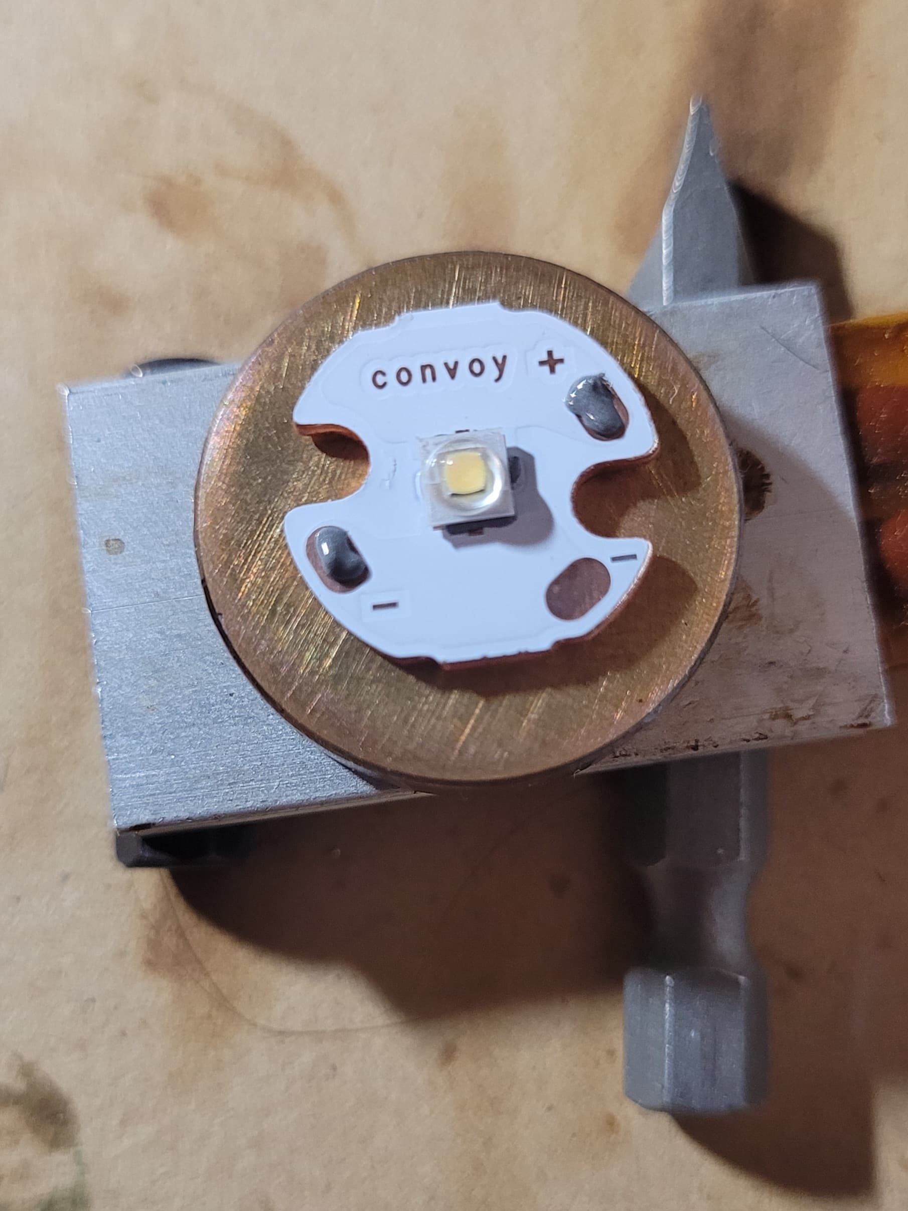
I see about removing the phosphor from flip-chip emitters. If one were to do this on an industrial scale, of course, it would be easier to start with royal blue emitters from Cree.
That sounds like a remote phosphor type setup, or maybe you meant having a mixture with high concentration of phosphor and only applying a thin layer over the die.
Maybe it is okay to not have the phosphor perfectly even: as we know, even domeless emitters still have the angular tint shift problem to some extent. If the phosphor is poured in such a way that is thickest in the center of the die and slightly thinner toward the edge, then the sideways emission will probably be less yellow, and the yellow corona problem should be solved. Maybe an ideal distribution of thickness can be calculated from the Lambertian model, but that sort of precision hardly matters in practice.
Also if we use a sealant that starts in liquid state, I can imagine the surface tension and cohesive forces of the liquid being helpful in evening out the phosphor pour, maybe even with a (possibly desirable) bulge in the center.
That’s what I meant, basically making paint with phosphor as the dye.
The problem with this is that you’ll have more blue emission on the edges, exacerbating the eggyolk effect of the hotspot present on some emitters like the GT-FC40 or some XHP70.3HI
To fix the sideways emission of light, you can use opaque black epoxy on a toothpick to “paint” the edges of the die. I’ve seen it done on BLF, IIRC it was a post from a very long time ago to some dedomed Cree emitter, might’ve been a sliced and diced XHP70.2
Thank you for the carefully edited images! With a standard HI emitter the hotspot is cooler than the corona, while in the pictures you sent the hotspot is warmer–it seems plausible that the ideal is somewhere in the middle.
The issue of egg yolk beam profile is two-fold: with the XHP.2 emitters, the main issue is the overpouring of phosphor past the edge of the die, which is corrected by dicing.
With standard HI emitters the issue is more complicated: as the viewing angle changes, the thickness of phosphor that blue light has to pass through increases as tan(theta) where theta is the angle away from direct, frontal emission. The increased “apparent” thickness of phosphor across the entire die is responsible for the yellowing of sideways emission, and for this reason I don’t think a fix that only applies to the edge of the emitter can fix the problem as a whole.
I’d like to know what emitters you’ve experienced that with, so I can try to get some, or look closer at those I have.
I’ve had nothing like that myself, and I have plenty of reflector lights with dedomed 519a and other domeless emitters (B35AM, SFT40, W2, SFS80, XHP70.3HI, FC-40, SBT90, etc). The only ones I notice tint shift on are those with an uneven phosphor pour/color (XHP70.3HI, FC-40), and/or side-emission of light (XP-L HI, XHP70.3HI).
Your explanation seems plausible, but I haven’t observed that phenomenon myself. As some people might put it, it seems like bulls*** but it’s good bulls***. Mostly I’ve just used my eyes for that though, taking measurements with my Opple LM3 or a spectrometer might reveal a small difference.
Either way, I’m pretty sure the ideal would be a perfectly even phosphor pour like that on the 719A or B35AM, as they have very consistent tint over angle.
A classic is the XPL-HI, though I don’t think I’ve ever experienced a single white emitter without any tint shift. Any domeless emitter should be a good example, especially in high CCT. Maybe the phenomenon is more noticeable with larger die emitters, with less edge effect.
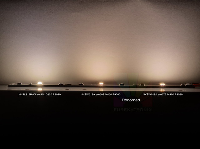
Whether you see tint shift on dedomed 519As might be a matter of sensitivity–I’m super picky and do notice it in real use. Here’s a beam profile comparison (source) of two dedomed 519As next to a 219B; you could decide for yourself. IRL I’d say the tint shift is more visible than in the photos, especially if my eyes are white-balanced to a warm CCT. One really annoying thing some cameras do is shifting tint when the intensity is changed, making low-intensity regions look more pink than they actually are, but this photo doesn’t seem to have that issue.
It’s very clear and noticeable on the 219b but that is due to the dome, but I don’t really notice it on the image, though it might be from the camera. There’s a tiny little bit on the edge, but that seems like it’s just the artifact from the silicone around the die.
I agree on cameras being annoying. The ideal approach would be to have an imaging spectrometer, but those are cutting-edge lab equipment and many thousands of dollars. Maybe a camera using an RGBE (red, green, blue, emerald) or CYGM (cyan, yellow, green, magenta) filter instead of RGB could capture it better.
No information about this company except from their own websites and social media accounts. Nothing that can verify their claims. Idk, I’m pretty skeptical about this one. I’ll believe it when I see it.
I totally forgot about the SFN60, I have my San’an emitters suffer from it, somewhat. SFN60 5500k is especially bad, the SFH55 is saved by virtue of being so blue that you don’t notice it (CCT is OVER 9000!!!)
I am also skeptical, looking at the datasheet spectra, that a 450nm pumped LED at over 5000K can achieve a R12 of over 90. But the fact that they explicitly listed lower bounds for R9 and R12 shows that they care about it to some extent, which makes it easier for me to suspend disbelief, at least for now. I can’t wait for the test results!
Ya I took the SFN60 5500K out of my D1k for that exact reason and replaced it with an SFH55 lmao
I don’t think mine is over 9000k but it might be. I can’t remember off hand. Think it might be like 8000K. But ya no tint shift issue. Very clean beam
These emitters remind me of the white XP-E2.
Upon release, the thermal resistance was at 8 to 9 °C/W, which is more or less identical to these Moonleds MN-S3535 (at least this is the name shown in the datasheet). Later the thermal resistance of the white XP-E2 was improved to 5 °C/W.
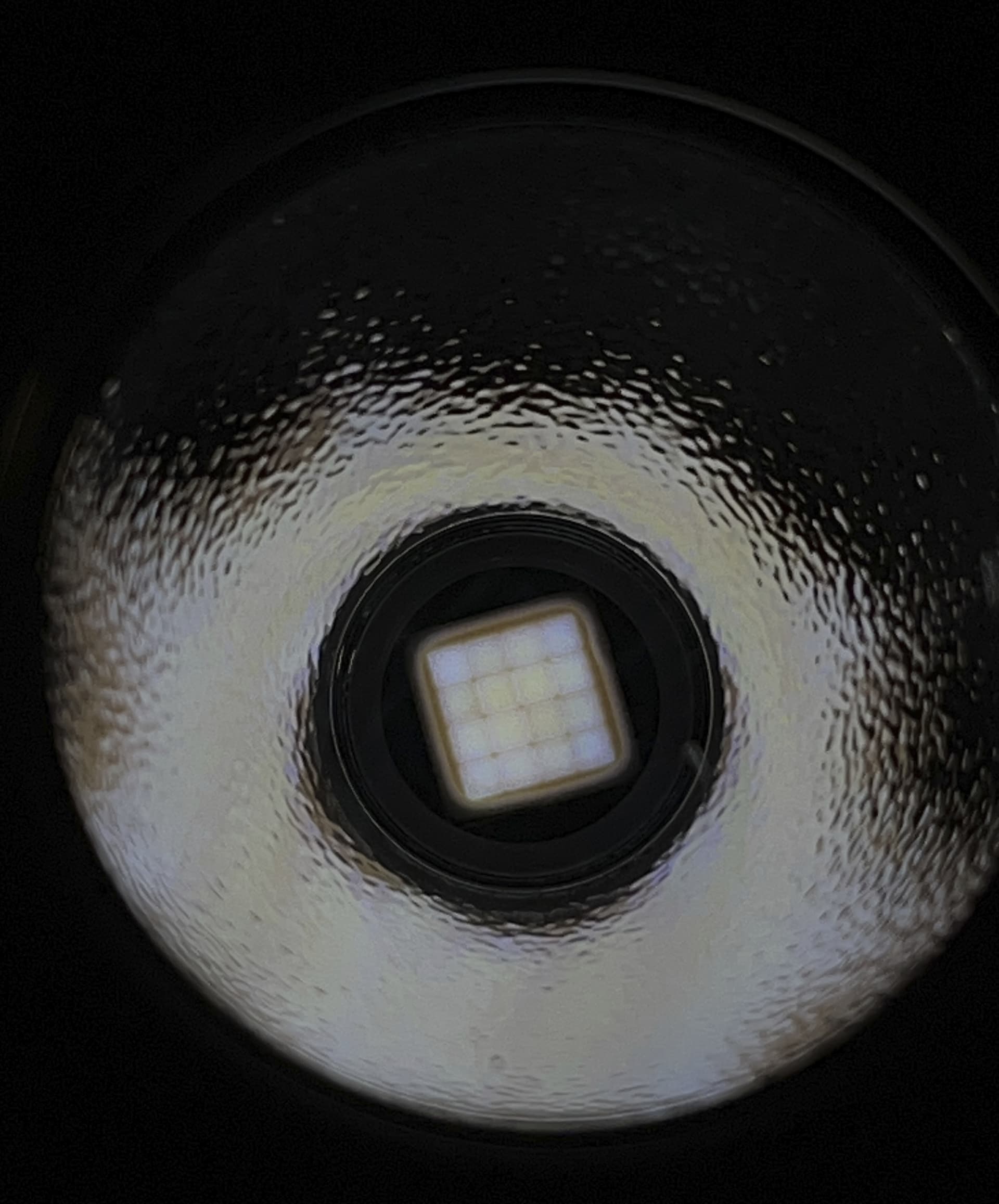
Maybe the LED chip is indeed very small and built like in the XP-E2 emitters. Although the orange luminous area looks relatively large, sometimes the phosphor has been applied to a larger area than the size of the chip (this was also the case with the Yinding 5050 95 CRI).
If so, a max current of 3 to 3.5 Amp is to be expected. This depends also on the Vf, but these are not high performance emitters.
This means that this emitter must score points with perfect light quality (color rendering, tint, light pattern for use with secondary optics) instead of performance.
Amazing!!! Have you gotten a chance to put it into a light yet?
The datasheet shows an LED with a much larger die, like SST20-sized, while the one received has a much smaller die. Not sure what the deal is here.
The zoomed-in images on the LED’s website do seem to show a bulge in phosphor pour along the edges of the square die; I think the slight overpouring is expected to eliminate sideways blue light leakage (which sometimes happens with SST20s).
Nevertheless, I doubt that the illuminated area of the LEDs that we have here for real in reality is smaller. I also have the impression from the picture in the data sheet that the illuminated surface is the same size in both pictures (data sheet vs. real LED), but the refractive index of the dome’s silicone may be different or misleading and the illuminated surface also appears larger or smaller due to the different angle of view and the different perspective.
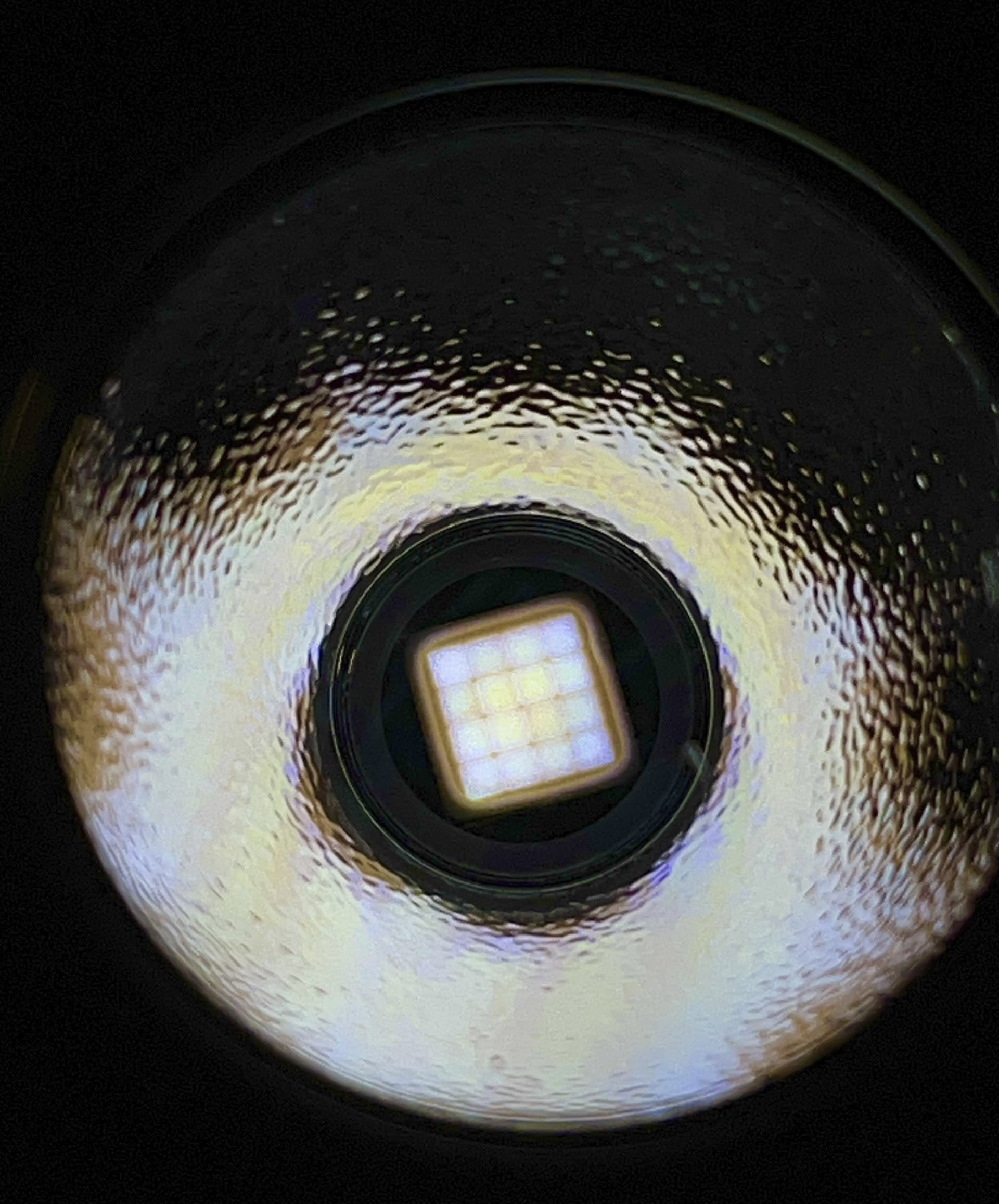
Maybe, but I also think I can recognize a kind of “round pattern” in the middle of the LES on the picture in the data sheet. Of course, I cannot say which chip it is exactly (round or square), but perhaps there is a round chip installed, maybe even the same one as in the SST-12. At least the thermal resistance and the similar presumed electrical characteristics would make sense. According to the data sheet, the SST-12 has a lower nominal thermal resistance (5.9 °C/W), but the performance of max. 3.2 A at 771 lm @ 3.49 V was still not as good as would be expected due to the thermal resistance.
It still appears to me that there are two different versions of the emitter floating around–the website shows two images, and one of them (the larger apparent LES) has a black substrate and a dot on the anode side, while the other one has a light-grey substrate and no dot. It looks like the no dot version was received.
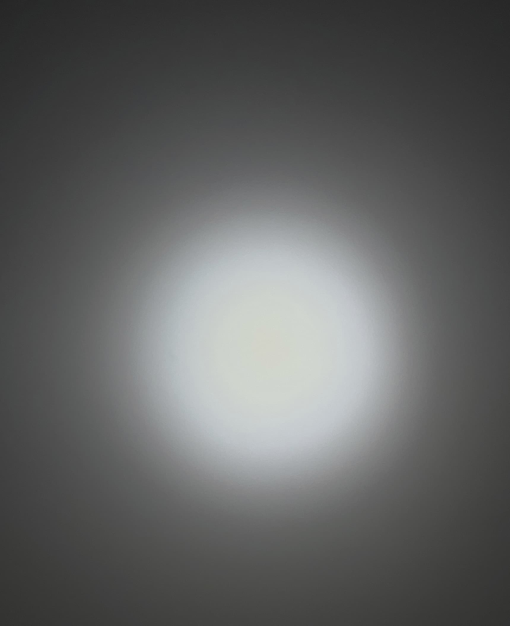
I really hope the die is not too much smaller than the phosphor pour, otherwise we will get the Cree rainbow typical of 2nd gen XHP emitters. In any case I’m very excited to see your test of this!
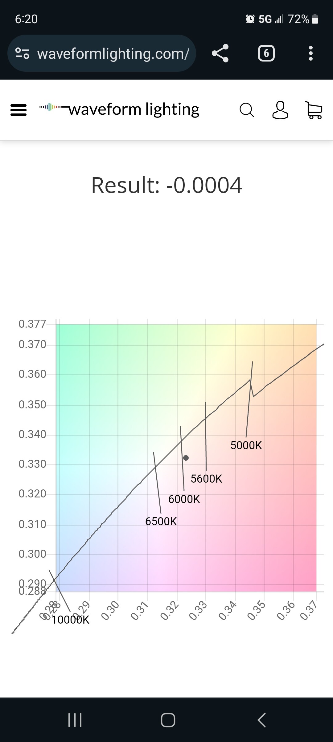
Insane!!! The 100Ra is really something, even within Opple’s error range. Too sad Opple doesn’t have a way to show R9 or R12. How does the 5000K one look?