I changed R1/R2 (still the build of post #1) to 330k/82k and that brought the current in off-state down to 11µA (0.011mA) with a cell that is 3.3V resting. With 33k/8k2 it had been ~68µA after the ADC_off() firmware mod. So in the end I’m down from ~200µA to 11µA which is very very good.
LVP is still working as before and triggering effectively at ~2.9V. But I’ll keep monitoring that. TomE, great help, the firmware changes made for the major part.
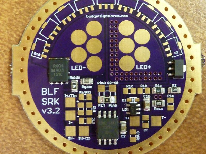
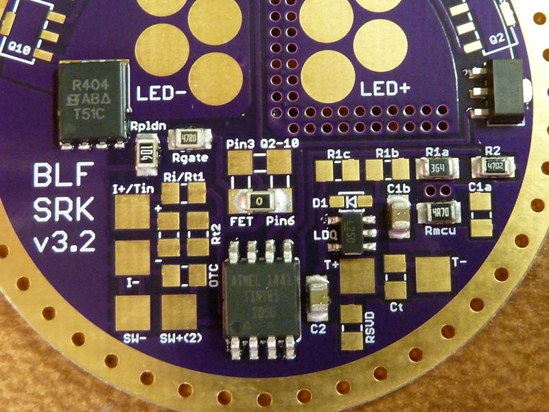
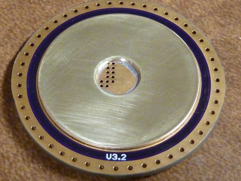
While at it I installed a 33R as series-gate-resistor (Rgate). Not sure if it’s needed, as the FET is not PWM’d, but it can’t hurt to have it in place.
HQ - just found out the LDO requirement is Vout on pin #5, not pin #3. That's an important spec, so I just found out. TA's LDO drivers are wired the same way. Think you got it from Richard's BLF SRK V2. Weird because Richard's other LDO drivers have Vout on pin #3. The LDO's I bought from Mouser, and one I got from Richard have Vout on pin#3, so of course there was smoke when I tested it . Fortunately the only thing that seem to smoke was the 4.7 ohm resistor, so easy to replace, but I have to wait on an order of LDO's with Vout on pin #5.
Forgot bout that thread. The wrong LDO I bought Richard used in the TK61 driver he designed, listed in the OP here: https://budgetlightforum.com/t/-/31955
Firmware has been tested. It's Narsil as the baseline. The table of voltage levels have been updated to support the 360K/47K R1/R2. It comes straight out of the spreadsheet I used to calculate them. It's conditionally compiled in, as below. The calculated values work very well now. Found a bug in indexing these ADC values where indexing was off by one. Not sure, but thought I got this code from somewhere else, maybe Bistro?
#ifdef USING_360K
// The ADC values we expect for specific voltages: 4.4V to 8.8V (2.2v to 4.4v). This is
//  for using R1=360K/36K, R2=47K/4.7K, and direct connection from Batt+
//  to R1, no diode in-between, with an LDO and a 2S battery configuration.
#define ADC_44     236
#define ADC_43     230
#define ADC_42     225  // 100%
#define ADC_41     220
#define ADC_40     214  //  75%
#define ADC_39     209
#define ADC_38     203  //  50%
#define ADC_37     198
#define ADC_36     193
#define ADC_35     187  //  25%
#define ADC_34     182
#define ADC_33     177
#define ADC_32     171
#define ADC_31     166
#define ADC_30     161  //   0%
#define ADC_29     155
#define ADC_28     150
#define ADC_27     145
#define ADC_26     139
#define ADC_25     134
#define ADC_24     129
#define ADC_23     123
#define ADC_22     118
#endif
That mod sounds good. Dunno bout anything else - I like all the versatility this driver offers. There's plenty of thru holes for Batt+, but I'd still like to do something more there, but not sure how. I'd like to be able to solder fill the thru holes but not sure if the holes are wide enough. Hard to see but the holes themselves appear to be covered in purple soldermask but I'd like to see the entire holes to be bare ENIG. This way solder filling should work well.
This is what I did for the contact surface:
Got from here: etsy.com brass-discs-20-gauge (might be cheaper direct from their shop: https://boppermetalsupply.com/) in 1 3/8" size that fit well. All I did was drill the center hole and sand it down to get it flat, then reflowed to the driver. Bad thing was I added the brass disc only after reflowing the parts, so didn't get the PCB heated enough to use hot air, so had to use a torch.
Brass is preferred (to me at least) because it's harder than copper and I don't think has as much problems for electrically conduction loss from oxidation.
The thru holes seem to have filled up with rosin and not solder paste unfortunately. If I were to do this again, I'd apply solder paste maybe on the component side and apply the heat on the battery side to see if I could fill the holes first, before reflowing the copper disc.
From the picture above, clearly the larger ground thru holes are not coated with soldermask. I didn't closely look at the Batt+ thru holes though - I might be wrong there.
Well, i meant a wall adapter 6V or 12V or a battery, whichever the LED works with.
So i wonder what changes are required on the circuit, a different LDO for example, and also in the code. Btw, do you mean “low voltage programming” by LVP?
Low Voltage Protection - the firmware logic to read the voltage level, and act on it accordingly if it's deemed to be getting low. We typically use two thresholds - one for a warning, and to drop output amps, then the next threshold to turn off LED output completely in order to save the cell from going below it's "safe" level. The two levels can be 3.2/3.0V or 3.0/2.8V.
Well, the board I built/shown in post #51 above has 2S (2 in series) Li-Ion input, so it gets from 6.0V to 8.4V input. It uses this LDO: https://www.arrow.com/en/products/mic5235-5.0ym5-tr/microchip-technology that supports up to 24V input, and outputs 5V, so it can handle a 6V or 12V DC source. If you want LVP, then the R1/R2 voltage divider resistors would have to be picked accordingly, and the ADC values to match - listed this all in post #51 for the 2S setup. This design though passes the source voltage along to the LED(s) - it doesn't buck or boost voltage to the LED(s).
Thank you for the explanations. Also, is this driver really capable of driving 16 x XP-G2? I’m guessing the max. current is solely dependant on the FET.
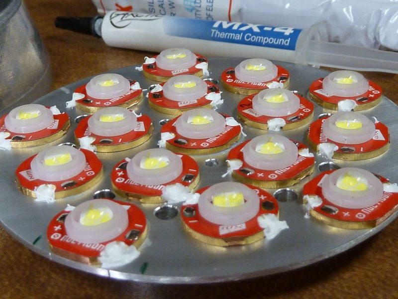
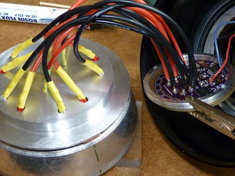
I'm using 16 XHP50's so it's a lot more power than 16 XP-G2's. The FET I chose, the SIR404DP is capable, but I'm having problems with the 7135. I added a grnd jumper to help in heat, and added a heat sync on top of the chip, and it's surviving now, but not working normally - delays coming on, sometimes doesn't come on at all.
Don't have time to trouble-shoot it further now. Might get back to it, or eliminate the 7135 altogether
PWM'ing FET's works great, specially at high PWM rates, but say for example you are getting 6 amps out of a FET on full, PWM'ing the 6A means you are pulsing 6A constantly. The way the 7135 works is it limits output to 350 mA, so to get 350 mA out, just drive it at it's fill capacity. So instead of continuously spiking 6A out, you get a smooth consistent 350 mA of output. This works way more efficiently than PWM'in a FET to get an equal amount of light output.
So we use FET+1 circuits/drivers for this reason. If you PWM the 7135, you get very efficient low modes, all the way from less than 1 lumen up to about 150 lumens.
Take that one step further like HQ did on this board design, add in a bank of 7135's and you get 3 output channels: 1 7135, bank of 7135's, and a FET. This way you get efficiency out of the middle modes as well, using the bank of 7135's. Wiring 7135's in parallel effectively adds them for total amps output. 8 7135's is 2.8A, 16 7135's is 5.6A, etc.
Bout that FET, there's a few things to look for. DEL and a few other BLFers could analyze the specs wayyy better than I could. I don't take the chance - I only use what's been reviewed, and then proven.
 . Fortunately the only thing that seem to smoke was the 4.7 ohm resistor, so easy to replace, but I have to wait on an order of LDO's with Vout on pin #5.
 . Wai'tn now for the LDO's.