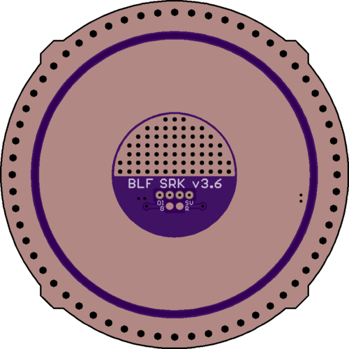
[Oshpark] BLF SRK FET v3 (46mm / LFPAK56 / Dual+Triple Channel / ATtiny13A+85)

Awesome!

So who do I need to talk to about getting one of these drivers made for me, I can solder the led and switch wires but dont think I trust myself to do the whole thing yet. Also would I be able to have “Narsil” or Toykeepers new ramping FW flashed on it for me? I have nothing to do that with.

One last thing, will I be able to do lighted switch?

I know Lexel is making some of the T_A drivers for sale. Maybe you could talk him into this?

Hhmm. Think I'm out of drivers, so if I order some, they come in 3's so I'd have extras. Yes - I got support for the lighted switch - actually mine is using the stock blue and it's a bit too bright, just haven't got a chance to tweak it. If you can wait a few weeks, I'd be able to build one up - doesn't take much more time from doing 1 or 2, or 2-3, etc.

Gentlemen,
long time no see

Tom, I knew this driver was in good hands with you. I’m truly impressed.
I implemented DEL’s C3/C4 and refined the design, see next post.
Have them in my hands already, looking very good, just no time for building…

Lexel, the temperature sensor is a direct implementation from RMM’s v2. I never used it myself, just kept it in the design. As far as I understand the sensor itself has 3 pins: T+ and T- are its power supply (hence T+ to the output of the LDO) and Tin is the sensed value. Tin is fed into the Attiny Pin3 through a 2-resistor voltage divider (Rt1/Rt2) to get the voltage down to a level the Attiny can evaluate (probably below 1.1V as for the LVP input at Pin7).

But now let me introduce you to v5.
I heard Photobucket is not the same anymore… Interestingly all my pics still show. I keep my fingers crossed, but I need to get a different hoster.

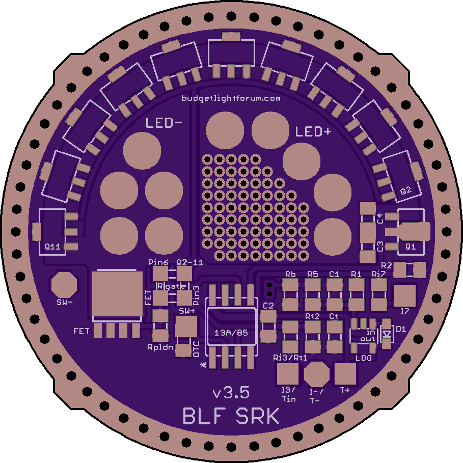
BLF SRK FET v3.5

.

Added C3 and C4
Rearranged LED+ vias
Still focus on High Current :wink:

.

https://www.oshpark.com/shared_projects/BFX7d296

.

.

Great to see that it’s still being actively developed! It looks good!

Del wrote place C4 as close as possible to the FET
I did that in my designs

Ah, hadn’t seen that he wrote that, thx.
Fortunately that is an easy fix.

I'm ordering as soon as the updates are ready . Glad I procrastinated on ordering the next batch of 3... I already got in another white MT-03 and don't have a driver for it yet.

Between the Infinion or the SIRA20DP, either is a great choice for these boards in a high performance light.

here you go :slight_smile:

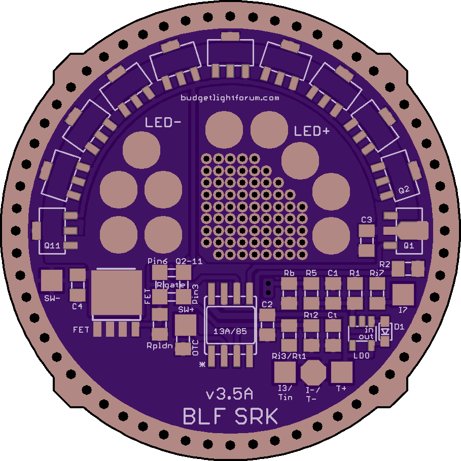
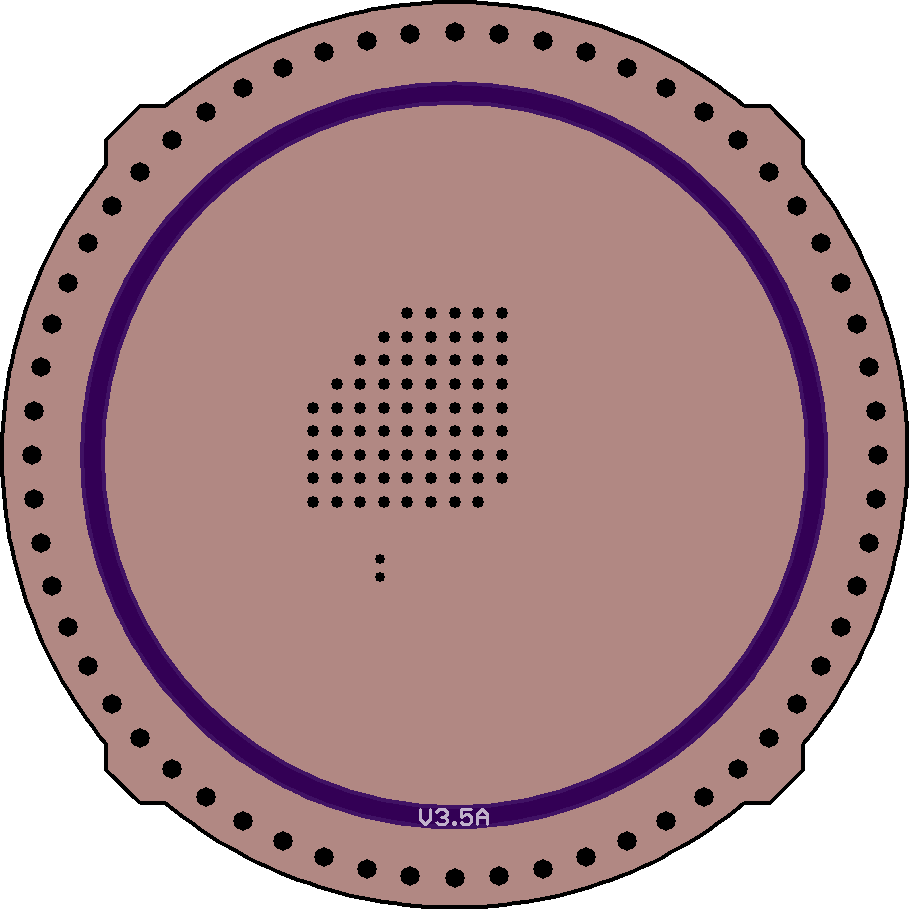
BLF SRK FET v3.5A

.

https://www.oshpark.com/shared_projects/LZhFeMG8

.

.

.

Schematic:

.

Pin5 is hardwired to the single 7135 (Q1) for the low modes.

Pin6 and Pin3 can, using the fancy 4-pad-connector (aka QuadPad), alternatively be connected to Q2-11 or the FET.
For the Attiny13A: use Pin6 for the channel you want to PWM, be it the FET or Q2-11. Use Pin3 for the channel you want to just switch on/off.

.

Component list:

- 13A/85: MCU ATtiny13A or 25/45/85; 8S1 (SSU) or 8S2 (20SU)

- R5: series resistor between VCC and MCU pin1; 0805

- FET: n-channel MOSFET at Pin3 or Pin6; LFPAK56

- (Rgate): series gate resistor; use the QuadPad (FET-to-pin3 or FET-to-pin6); 0805

- Rpldn: pulldown resistor (gate to GND); 0805

- Q1: single AMC7135 at pin5; SOT-89

- Q2-11: up to 10 AMC7135 at pin3 or pin6; SOT-89

- D1: schottky diode (~0.25V) for 1S (4.2V); SOD-323

- LDO: low dropout regulator for 2S (8.4V) [LDO needs C1 and C2]; SOT-23-5 (Vout is pin5)

- C1: input capacitor between VCC/LED+ [behind R5] and GND; 0805

- C2: decoupling capacitor for MCU; 0805

- C3: additional capacitor between VCC/LED+ and GND; 0805

- C4: capacitor between drain/LED- and GND; 0805

- R1: voltage divider to VCC [before D1 / behind R5]; 0805

- R2: voltage divider to GND; 0805

- Rb: bleeder resistor from VCC to GND; 0805

- SW+: pad for momentary switch to pin2

- SW-: pad for momentary switch to GND

- Tin/Rt1/Rt2/T+/T-/Ct: temperature sensor

- I3/Ri3/I-: indicator LED at Pin3

- I7/Ri7/I-: indicator LED at Pin7

  • OTC: offtime capacitor for clicky firmware [using SW+]

Notes:

- Q1 can be used as Nanjg star 2

- Rt2 can be used as Nanjg star 3

- OTC can be used as Nanjg star 4

- a zener can be placed on Ct, which is MCU+ to GND

  • a momentary switch at Pin3 can be soldered to the QuadPad

Ordered! Thanks!!

Ooooohhhhhhhhh.

A first look at the next version.

Goal is to implement programming while maintaining high current capabilities. I will go with the “jester” design, simply because it’s more space-efficient.

.

.

In v3.5 the MCU was much more below the center and I really don’t want the cells to short with the ground via of the programming pad…
So the MCU had to go up, while the BAT+ vias should as well be out of reach for the cells. Really don’t want the cells scraping these vias. To keep as much BAT+ vias as possible, they needed to be distributed sideways… and the rest just fell in place.

Advantages are really fat current paths, be it from the ground ring to source, from drain to LED, from the cells to LED and for all AMC7135, where the route widens with the amount of 7135s. And having the output path of the 7135s not under them allows for larger ground pads of all 7135s.

.

Some finetuning needed and it should be ready.

could we please agree on one programming key standard?

why now make a 2. with different footprint and pin orientation?

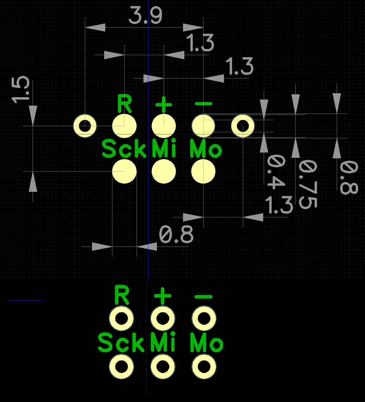
2 examples of course depending on driver minimum is 2 viases and total of 6 pads and if possible no conducting parts left and right in the upper row, even if on latest I insulated on the key those pogos from ground

you can use your key on my footprint without any modification, reverse it does not fit

a)
this SRK driver
Ah, you disconnected your orientation pins from ground, that allows some interoperability and avoids the short between VCC and GND.
I can make this driver dual purpose to fit your key as well.
It’ll loose orientation protection but I trust those who build this one know what they’re doing.

b)
key standard
I can’t give us a common standard because I will not use a single standard even on all of my own boards.
I thought I had explained in my progkey thread. Will try again:

I tried your pin distribution (3+3 with VCC down center) on several of my drivers and it did not work well. Simply impossible on one, difficult to route on others. Your orientation pin is where the VCC via will be, much better to use it just there. And I want more vias, preferably all of them, the contact on pads sucks.

Don’t get me wrong, the idea of a programming key is fabulous and I’m absolutely grateful you introduced it on BLF with ways for a practical solution. I’m so giddy about this that I did more driver developing in the last month than in the whole rest of the year. A bit like when the OTC was introduced. Major Step. A Real Thing.

So I tried different approaches and I saw that I don’t want to limit even myself to a certain layout. There’s one layout I prefer, but I can’t get it to work on all boards. So these became my priorities:

- as much vias for the pogo pins as possible (preferably 6, for good contact)

- least possible routing for the prog part (often the space is already needed for the driver circuit)

  • avoid wrong orientation, so no symmetry up and down

So I made the 4+4 progkey that allows all this, is universal, small, dirt cheap and easy to build.

You know, these are all drivers I use myself, highly customized, some for just a single type of flashlight. Some have 1s/2s and double/triple channel selectable on one small PCB. I want to keep the freedom to use the best programming pattern for each driver. That’s why I chose a flexible approach, and shared the progkey to use it. I simply share what I use myself. Anyone who wants to use it, can freely do so. It’s my way of giving something back to the community.

Those who use your drivers can use your key. That’s perfect. And I really suggest they do, because that way it’s foolproof!

And the small handful of hardcore DIYers that really build my boards, well, for 4 bucks and change they get 3 progkey PCBs from Oshpark and 100 pogo pins from Fasttech and can program all they need.

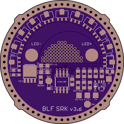
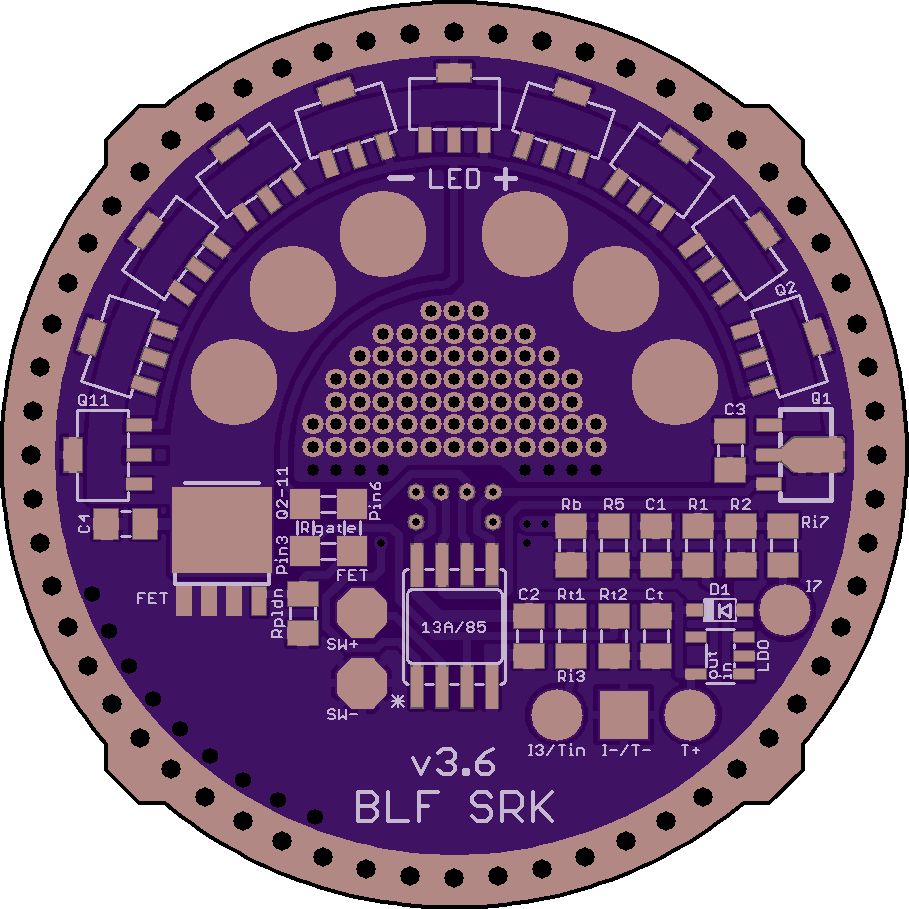
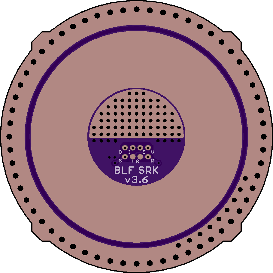
BLF SRK FET v3.6

.

Same circuit, but some major overhaul.

Added Vias for a Programming Key to allow for programming while the driver stays in the light.
Performance optimizations: Even more LED+ vias, more GND vias around the FET, wide path from GND to Source
LED+ vias still unmasked to allow filling with solder and all vias are inside the battery contact circle
LED pads reduced to 2x3, but each pad increased in diameter
Unified the other pads: octagonal for both switch pads, round for I3/I7/Tin/T+, square for I-/T-

Honestly, can’t wait to get these into my SRKs :smiling_imp:
.

https://www.oshpark.com/shared_projects/LZhFeMG8

.
.
.

Schematic:

.

Pin5 is hardwired to the single 7135 (Q1) for the low modes.

Pin6 and Pin3 can, using the fancy 4-pad-connector (aka QuadPad), alternatively be connected to Q2-11 or the FET.
For the Attiny13A: use Pin6 for the channel you want to PWM, be it the FET or Q2-11. Use Pin3 for the channel you want to just switch on/off.
Mind that the position of the pads within the QuadPad has changed due to the optimization of the driver.

.

Component list:

- 13A/85: MCU ATtiny13A or 25/45/85; 8S1 (SSU) or 8S2 (20SU)

- FET: n-channel MOSFET at Pin3 or Pin6; LFPAK56

- (Rgate): series gate resistor; use the QuadPad (FET-to-pin3 or FET-to-pin6); 0805

- Rpldn: pulldown resistor (gate to GND); 0805

- Q1: single AMC7135 at pin5; SOT-89

- Q2-11: up to 10 AMC7135 at pin3 or pin6; SOT-89

- R5: series resistor between VCC and MCU pin1; 0805

- D1: schottky diode for 1S (4.2V); SOD-323

- LDO: low dropout regulator for 2S (8.4V) [LDO needs C1 and C2]; SOT-23-5 (Vout is pin5)

- C1: input capacitor between VCC/LED+ [behind R5] and GND; 0805

- C2: decoupling capacitor for MCU; 0805

- C3: additional capacitor between VCC/LED+ and GND; 0805

- C4: capacitor between drain/LED- and GND; 0805

- R1: voltage divider to VCC [before D1 / behind R5]; 0805

- R2: voltage divider to GND; 0805

- Rb: bleeder resistor from VCC to GND; 0805

- SW+: pad for momentary switch to pin2

- SW-: pad for momentary switch to GND

- Tin/Rt1/Rt2/T+/T-/Ct: external temperature sensor

- I3/Ri3/I-: indicator LED at Pin3

  • I7/Ri7/I-: indicator LED at Pin7

Notes:

- Rb is parallel to C3 and can be used to add capacitance

- Ct is parallel to C2 and can be used to add capacitance or for a zener diode

- Q1 can be used as Nanjg star 2

- Rt2 can be used as Nanjg star 3

- SW+/SW- can be used for an OTC or as Nanjg star 4

  • a momentary switch at Pin3 can be soldered to the QuadPad
reserved for application examples

That’s a really nice looking board. It’s nice having all those easy to find pads for temp sensor and indicator LEDs, as well as the programming vias/pads and all the other great features.

EDIT: I saw your post in Mike C’s GAW thread. Seeing this new board design, I’m wondering whether you have any intention of moving to more advanced MCU chips in the near future, or if you think ATtiny85 is good enough for your purposes for the foreseeable future.