Because these boards have no ground ring and are intended to 'float' above the host driver, they need all 4 connections connected in some form or another. So the way I would do it, is thus (motherboard refers to the existing driver):
1) Connect LED+ of the 'motherboard' to LED+ of the slave, and the LED+ of the slave to the LED.
2) Connect LED- of the 'motherboard' to LED- of the slave, and the LED- of the slave to the LED.
3) Run a wire from the PWM pin (or a VDD pin of an AMC chip) from the 'motherboard' to the PWM pad of the slave.
4) Run a wire from a GND pad (or GND pin of AMC chip, or even the host somewhere) to the GND pad of the slave.
All 4 pads have been made through hole because the LED+ and LED- pads need to run through to the LED anyway. The GND pad can go to the host of the 'motherboard' provided it's a shared ground. PWM...no particular reason other than to look neater lol.
A board is slaved when the chips on the second board are controlled by the mcu of the parent board. The out puts can be tied together to increase the current supplied to one led( up to battery output capacity) or they can be run separately to different LEDs and each led will be fed by however many 7135’s are tasked to it.
Question, if master and each slave boards were going to feed individual emitters could each individual board have a non shared battery? That way, say you could have a 3 cell / 3 emitter light and if you only had one battery in it only the one emitter would run.
Or is that not possible and you’d have to have the cells all together in parallel and all the drivers/emitters also in parallel connected together?
And if that is possible would you be able to control the master with a clicky switch and have the slaves be able to sit with power applied but turned off or again is it just not possible?
This should work. You have to use 3 slave boards and just one MCU board. The slaves all have their own battery, and the MCU is fed off ALL THREE batteries. The slaves all share the PWM signal from the MCU. This way, you can lose one battery and the MCU will continue to run, thus allowing you to still control the remaining two LEDs. If you did it any other way (for example one master board with MCU and AMC chips on it, and 2 slaves) it would not work. Or rather if you lose the battery that was powering the MCU board, none of the LEDs will light up.
If the MCU board has the batteries connected in parallel then there’s an electrical path between the 3 batteries unless you use diodes. You’d have to do that in order to prevent the batteries balancing. Low voltage protection is also potentially an issue depending on implementation. The ATtiny13 does have 3 ADC channels though, so I guess if you were determined you could make it work.
What do you mean exactly by current limiting? I don't want to limit the current - thought that was the idea of this FET design? Wondering now because a FET driver I built up for OL could not get full power, so he piggybacked resistors on the 100 ohm, then was able to increase power. Thought the resistor simply fixed mode switching issues?
Wait...what board are you referring to, and which resistor? The only 100ohm resistor I am aware of is the gate resistor (between the MCU and the gate of the FET).
BLF15DD, BLF17DD, and BLF20DD - in the OP, under the BLF15DD and BLF17DD it clearly mentions a 130 ohm resistor, while for the BLF20DD it's not mentioned.
The OP has 130 ohm listed while the OSHPark project postings clearly list 100 ohm -- they are different, conflicting...
I'm guessing it doesn't matter??
More Questions:
-- for an e-switch setup for the BLF17DD, I have to wire the switch directly to a MCU pin? No pad (star pad equivalent) like we have on the standard Nanjg? Was this an over site or no room?
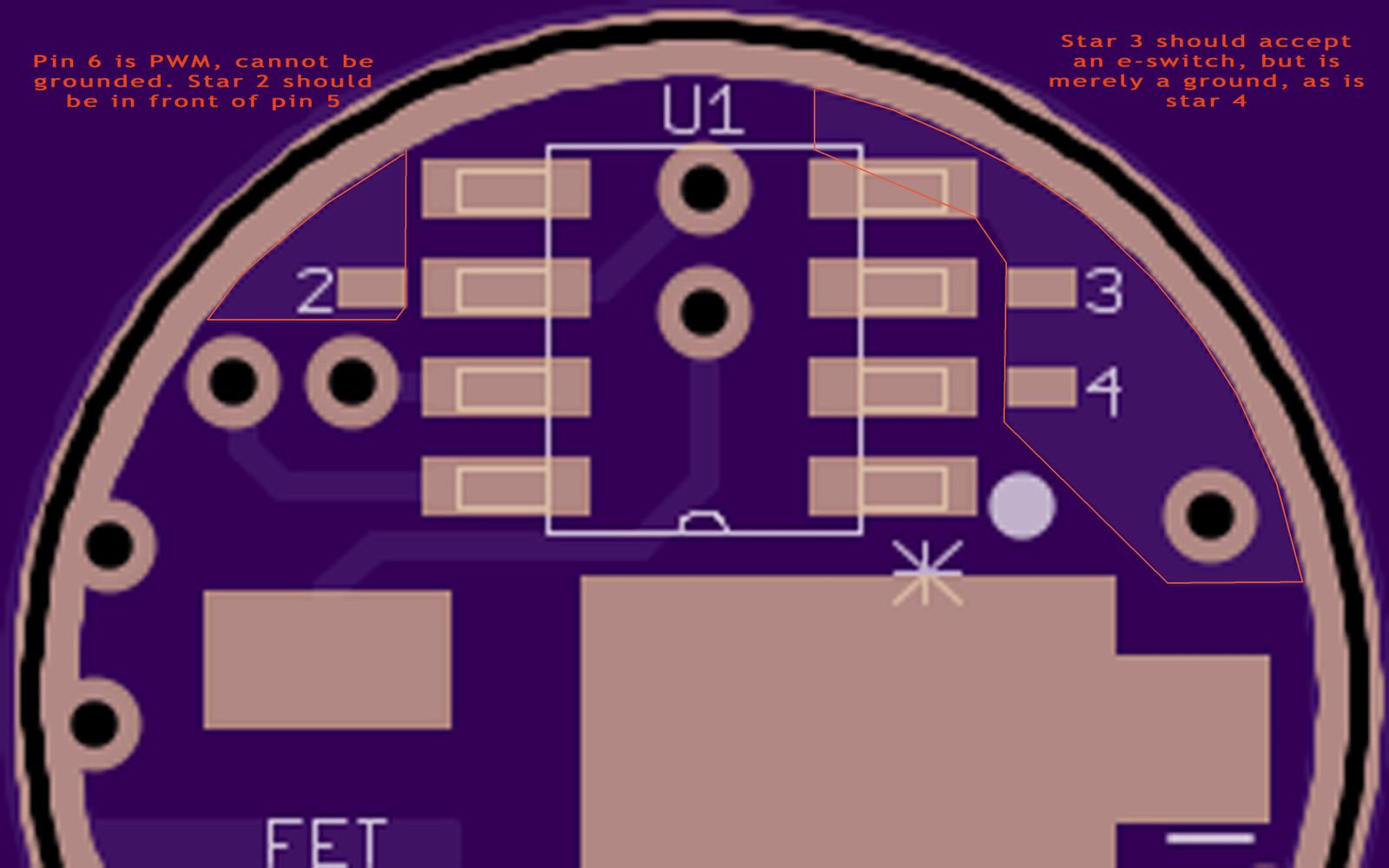
-- what exactly is the purpose of those 2, 3, and 4 pads? They seem to be connected to ground? Are they useless for an e-switch switch input? Why aren't they documented somewhere easy to get to?
-- I sure wish there was one simply place I can get info on each board so these questions don't have to be asked??
Hey Tom, on the original 105c drivers the star is an extension of the pad where the mcu’s pins are soldered and the stars are located beside the ground ring making it easy to ground that particular pin for the desired result.
On these smaller more compact boards, the star is a ground that is placed close to the actual pin to make it easy to ground the pin, there’s just not room to do it the other way. So if you’re hooking up an electronic switch, it has to solder directly to the mcu pin appropriate to that driver.
On the BLF17DD, star 2 is in front of pin 6…it doesn’t go with pin 6 but pin 5! Since pin 5 is right beside the ground ring it’s probably easier to ground it to the ring to get a moon mode activation with STAR firmware.
I don’t have the other driver boards, but have encountered the above as described.
I don't use the standard STAR firmware - just want to get a e-switch wire to pin #2 of the MCU - was hoping for a pad on the MCPCB so I don't have to remove the wire to re-flash firmware. I was browsing around and it looks like comfy has to do the same thing (solder direct to the MCU pin), so it is what it is I guess.
If only the layout/design would have had a pad for one of the 3 available pins, then at least for e-switch setups, it would make life a lot easier. Actually with that pad labeled "4" right by pin #2, it makes it harder to wire because you have to be sure you don't make contact to it -- yikes!! Haven't tried this yet. I'm thinking now the FET modified Nanjg is easier than the BLF17DD - I was thinking the opposite...
Let me clarify -- I never use driver firmware with soldered star options, ever... I always change the firmware to change mode configurations. So for me, it looks like I have no use for the 2, 3, and 4 pads on these board designs. In fact for me, it seems like they are more a hindrance than a help because they get in the way, being so close to the MCU pins. For now, all I have a need for is an e-switch input, which can be on any of the 3 available pins - I can easily change the firmware. I can understand my use is probably the exception not the rule, so no blame here -- I'm just trying to point this limitation out, now that I think I understand it.
The 2, 3, and 4 pads ARE connected to pins on the mcu. They do not match up to the pin number though. Look at the oshpark pictures of the boards and you can see the traces. I'll post something better in the morning.
Do you know if the ATiny13 can use the same .hex file as the ATiny13A? I wasn’t paying attention when I ordered the parts list for the Knucklehead…
And the star pads on the BLF17DD are simply grounds, not connected to the mcu pins. I found that out the hard way and had the PWM grounded out by soldering star 2 to pin 6 (which it’s right in front of) The star is just a ground pad, an extension of the ground ring not of the mcu pin. Or that’s the way it is on the 54 boards I have.
Do I need to edit the op for the DD boards or is it the carts that don’t match? The 15DD is the only board that has actual limit resistor pads between the FET and the LED and the value and wattage of that resistor are defined by the desired drive current. I’m guessing most will just jumper this with a wire.
Edit- I see, the resistor differs in the cart and the Oshpark board listing. I thought either value was ok.
When I do my 17DD’s for an e-switch I cut the ground trace around the top, bottom and right side of pad 3 so it’s no longer ground then I solder a tiny jumper from the MCU pin to the pad so I can solder the switch wire to the pad. Using a single strand of wire keeps things low-profile enough to still re-flash the MCU.
Edit: I don’t have any but I bet that conductive glue would work pretty well for the connection too, you’d just want to solder the wire to the pad first.
I was going to suggest something like that for TomE but you beat me to it.
So for the purposes of reflashing and e-switch connection it would be better to extend a trace from the pin pad towards the ground ring to shift any jumpers away from the mcu and have a possible e-switch connection shifted as well?