sure…inbound
Guys just posting an FYI about the new AO3400A FET’s, the old IRLM2502’s are not your standard SOT-23 package, they’re “SOT-23 Micro3”, they’re about 1/2 the size (front to back) of a true SOT-23. What that means is if your boards are really crowded like some of my 4Ch RGBW ones you may not be able to fit the AO3400’s even tho they fit on the same pad’s because their bodies are larger. The leg’s still fit (you may need to squeeze them a little) but the t/bplace outline is NOT large enough so if you’re wanting to use them make sure you leave more space or even edit your SOT-23.lrb part (or make different SOT-23 Micro3 and SOT-23 standard parts all together)
I thought they were the SOT-23-3
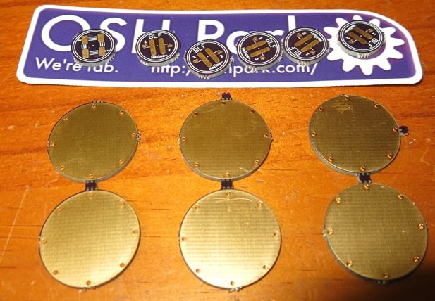
I got the footprint for the BLF15DD from a .lbr repositor, not sure was maybe adafruit or something like that
Correction…on Digikey
AO3400A - Package / Case - TO-236-3, SC-59, SOT-23-3
IRLML2502PbF- Package / Case - TO-236-3, SC-59, SOT-23-3
The TO-236-3 looks to be the bigger brother of the SOT-23-3
TO-236-3

SOT-23-3

Looking at the images on digikey though…they do look bigger

dang…that just sux so much…jeez
Here’s the pic I took on request of the DK CS lady

AO3400A on left, IRLM2502 on right.
C_K, re: "floating" board with 7135's. You probably are already on it, but just in case. You will probably need a thermal path for that raised board.
The fact that the center of the oshpark renders are black means there is no solder mask there. It should be purple. I'm not even sure what black means, but the machines certainly didn't know what to do with it!
I have asked the question so we'll see what they have to say. Maybe they are right?
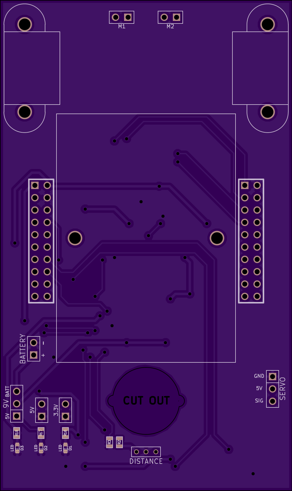
It could be a mistake on my part, but the boardoutline.ger looks similar to the one for the 26mm contact board… so I’m not sure whether it’s my problem or not. Neither cutout looks like they recommend, so maybe I should change my ways. Maybe I see what I did wrong. I’ll talk to tech support and ask to find out for sure, but maybe all I need to be doing is putting that text there for the cutout. A live person touches the gerbers before they go onto the equipment.
I personally can’t stand dead people handling my Gerbers…
Did you have “CUT OUT” in the middle? Text in the board outline layer.
I think you need to label the part you want “cut out ”
Like this
Ouch!
So what’s the difference between milling, dimension, and outline layers and which one do I draw the outline on? Right now, the dimension layer shows the drills but not the vias or the outline(drawn in milling).
… … … I linked to the support page in my post, I said that my slots didn’t look like the recommendations, I said that I needed to put the text there… Clearly I did not put the text there previously as it’s not visible in the OSH Park images. FYI it’s still possible to get a cutout without the text - as I tried to indicate previously it’s just for a human person to see and understand when they program the machine. (It was still my mistake to leave the text out though.) Without the text there’s a higher chance that the person won’t notice or do anything about your slot. I’d say that’s why in one case MRs_DNF received cutouts and in another case he did not.
I did read the support article before doing the cutouts, it’s simply that I forgot that the callout was needed by the time I was done. Anyway I just needed some time to think about it: no need to contact tech support, that entire thing is done incorrectly. Looking at the gerbers it appears that I used a 100mil path which forms a closed loop. That’s a no-no. I’ll have to go back and look at the BRD but I think I’ll need to re-do those things.
I just copy Mattaus and do mine on the milliing layer. Really the Eagle layer doesn’t mean squat though - you put the Eagle BRD through the CAM processor in Eagle and that determines what goes into what Gerber (typically multiple layers are condensed into single Gerbers, lots of stuff ends up on the top and bottom silk, multiple things might end up in the board outline, etc). If you open the CAM processor and load something like CAM job OSH Park provides you’ll quickly and easily see what I’m talking about.
Both of your links go to OSH Park ~, I didn’t know you saw the cutouts support page. I’ve had oshpark not render boards correctly at times. To me, not seeing “cut out” on your board didn’t mean its not there.
I’d heard talk of the Zombie apocalypse and I have Gerber knives. Bad timing I suppose. My apologies.
Have you guys noticed the speed difference between ordering your own uploads and ordering a shared project, this week I received boards (I uploaded) that I ordered on the 19th, I’m still waiting on a set of boards from a shared project I ordered on the 13th.
Have you checked tracking? A set of mine was misplaced by USPS for a week.