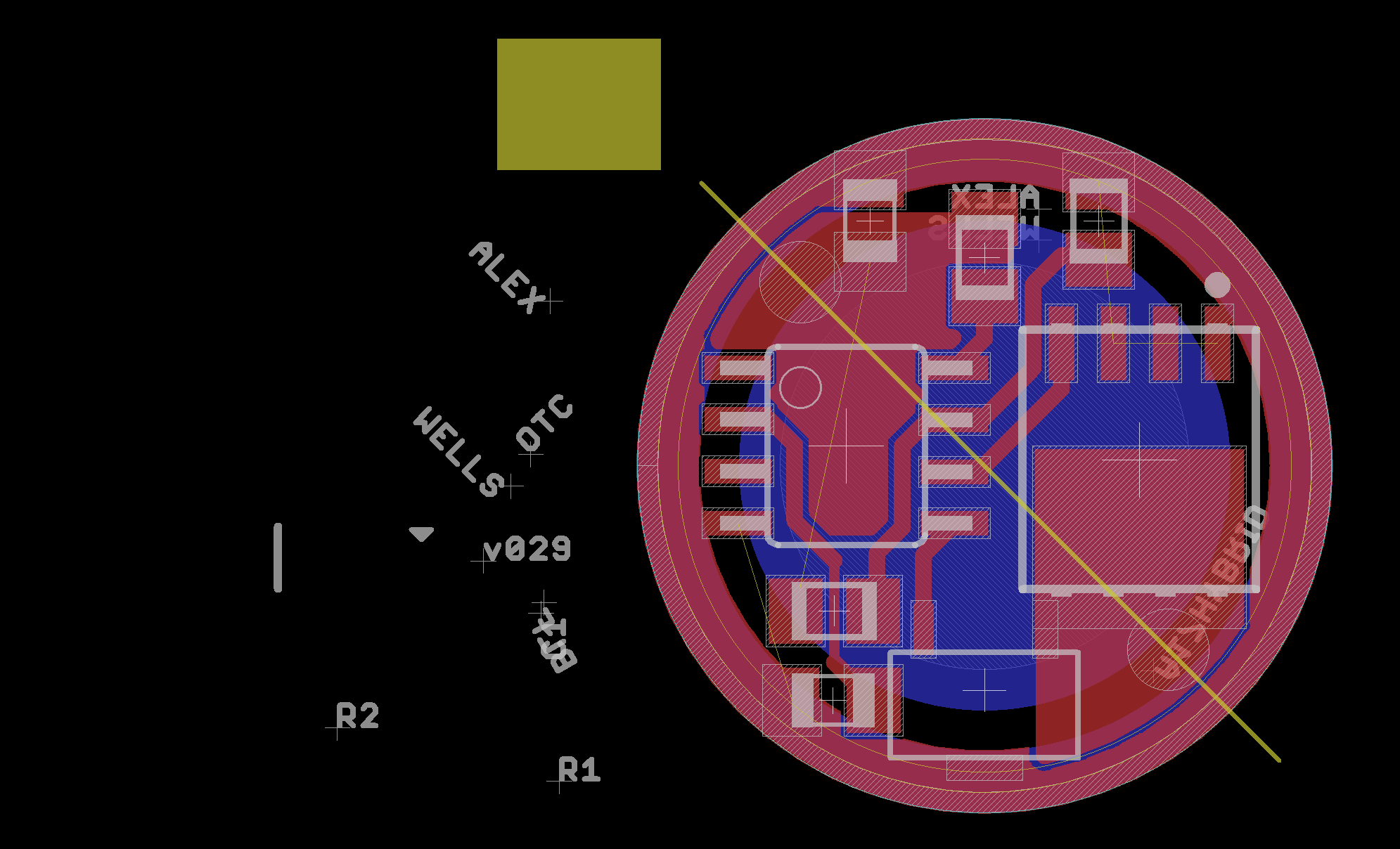
I’ve worked on this before and the layout did not work decently. In the past I depended too heavily on the LFPAK outline I grabbed from the internet. When I saw RMM take a crack at the problem (#3441) the truth is I initially dismissed his work: I thought to myself “shows what he knows, that stuff won’t fit.” Later the idea kept rattling around in my head again and it occurred to me that both RMM and I have built the A17DD-SO8 drivers and know exactly how much space each component needs. Clearly I needed to reconsider. Knowing how large the actual components are once installed on a driver like this makes a difference (as one might imagine :p).
Features:
- 0.5mm component keepout around edge. I may trim this up to a larger number in future revisions…
- FET + 1*7135: alt PWM is hooked up to the single 7135 so it may be possible to get this working with an unmodified version of STAR.

- No Zener! Sorry MT-G2 folks, you’ll have to stack a Zener
across C1 orbetween D1 and R2. Or maybe kind of wedge it between R2 and the FET. - Offtime ready.
- Large 1.5mm GND ring on bottom and on top (where possible). Exposed copper is 0.5mm on top and bottom.
- Like some other recent drivers, this driver does have a reverse-polarity protection diode but bypasses the diode for the voltage divider. Due to this we are able to use any diode desired. Ideally we use a protection diode with as low a Vf as is reasonable.
- The exposed spring pad is 10mm. Total pour diameter is 12mm.
- LED +/- pads are 2.0mm in diameter. They’re on much larger pours and diagonally across from one another.
- Some symmetry & stuff here and there.
v003:
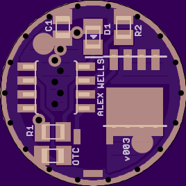
https://oshpark.com/shared_projects/I16olxS2
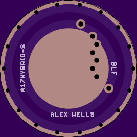
v002 WIP screenshot (just for show-and-tell):