You’re doing both the R and G with a single PWM?
No, it’s not using PWM at all for those… so it works just like the two banks of 7135s which would be completely on or off on the driver in the OP. The attiny13 only has two PWM outputs, and they’re already used for the FET and one of the three sets of 7135s. So, the other two are all-or-nothing.
In other words, the red+green LEDs only have a few discrete states: red, orange, green, dim red, dim orange, dim green, off. Technically it could also do dim on one and bright on the other, but that isn’t visually distinguishable from just the bright one alone.
Unless I’m wrong (and I could TOTALLY be wrong :-D) this gap actually wouldn’t exist.
Let me add a couple of rows to my hypothetical 2D array:
(single7135, dual7135, triple7135, FET)
(8/255,0,0,0/255) – terrible moonlight
(100/255,0,0,0/255) – brighter moonlight, heh whatever ![]()
(255/255,0,0,0/255) – 1*7135
(120/255,1,0,0/255) – ~1.5*7135
(0/255,1,0,0/255) – 2*7135
(0/255,0,1,0/255) – 3*7135
(120/255,0,1,0/255) – ~3.5*7135
(255/255,0,1,0/255) – 4*7135
(0/255,1,1,0/255) – 5*7135
(255/255,1,1,0/255) – 6*7135
(0/255,0,0,255/255) – FET Turbo
Adding in only 1 7135 between modes will likely not look 'right' (once you get up out of the lowest levels using PWM on the single 7135). Is this intended mainly for clicky or momentary control? The number of modes needed for good spacing could get kinda... clunky with a clicky UI. Momentary it would be less of an issue.
Another thing, will the 7135s add anything at all once the FET's turbo is active? Some of those little LFPAK thingies have stupidly low Rds.
Perhaps I misunderstood something. Is the setup like this?
- 1x7135 — w/ PWM
- 2x7135 — on/off only
- 3x7135 — on/off only
- FET — w/ PWM
So, ignoring the FET for now… the output ranges would be:
- 0mA to 380mA (smooth): ramp the 1x7135 circuit
- 380mA to 760mA (jump): turn off 1x7135, turn on 2x7135
- 760mA to 1140mA (smooth): 2x7135 on, ramp the 1x7135
- 1140mA to 1520mA (smooth): 3x7135 on, ramp the 1x7135
- 1520mA to 1900mA (jump): 3x7135 on, 2x7135 on, 1x7135 off
- 1900mA to 2280mA (smooth): 3x7135 on, 2x7135 on, ramp the 1x7135
The gaps would go away with the PWM on the 2x7135 channel… but it would also incur a cost of making the overall ramp not very smooth. It’s unlikely that 1x7135 + 127/255*2x7135 would actually have the same output as 255/255*2x7135… but this would only matter if it had a smooth ramping mode.
In all cases, the FET could fill in the gaps, but it’d be finicky and inefficient.
What I’m talking about seems really simple to me, but the way you guys are talking makes me feel as if I may be missing something.
I intend to use a 2D array in order to change multiple settings per mode - lots of settings. In the example I’ve given in post #34 the number of settings is 4 per mode: The status of PWM on a single 7135, the binary on/off status of a pair of 7135’s, the binary on/off status of a trio of 7135s, and PWM on an FET. Manipulating those four settings simultaneously (and arbitrarily!) for each mode should be straightforward: we just dump through a loop which parses each setting and sets the output accordingly.
Doing that gives us total flexibility, ToyKeeper that’s where I feel like I may have lost you. It’s a 2D array. A 2D array is like a table: it has rows and columns. If the columns are fixed (for this driver they are the four settings I described above) then to “create” modes we just need to fill in a few rows of settings. Since we are controlling all 4 outputs simultaneously and the gap between 1, 2, 3, 4, 5, and 6*7135 is never greater than 1 we can fill in between any of those positions using PWM on the single 7135. Thus there is no gap in any position.
I have no intention of implementing a smooth “ramping” mode. Clearly that’s not gonna work here, I’m confident that we CANNOT implement a nice version of something like this.
comfychair: I’m not sure I understand what you are getting at unless it has to do with a continuous-ramping mode. Of course the mode spacing will be correct. For H/M/L it could be something like 6/2/1*7135…. if anybody wants to tweak that they can use PWM as I described earlier in this post. If you’re saying that PWM on a 7135 doesn’t generate linear output then you’re certainly right, but I don’t see how it’s a problem unless we were attempting to show the user a continuous-ramping mode (which would look terrible and notchy). We should be able to generate a greater resolution than is available with a 6*7135 Nanjg 105c, so it sounds like an improvement over the status quo.
The 7135s will certainly achieve nothing while the FET’s turbo is active. They are only there to give regulated and PWM free modes.
Hopefully I expressed myself better this time. I’m sure some of it will come off as pedantic but I don’t know where the breakdown in communications is. It could certainly be me failing to comprehend the questions, but if that’s the problem you’ll just have to tell me.
If after all that explanation there’s still a good reason to put PWM on the 2*7135 instead of the 1*7135 please try to figure out a way to tell it to me / explain it to me ;-). Thanks for the input folks.
EDIT: To be clear, she lost me. Oops! Strikethrough added for clarity on that subject. See my next post.
Oops ToyKeeper, my mistake. I see that you’ve got it down pat in your post #36. IIRC my original concepts had two single 7135’s, avoiding the two jumps you’ve pointed out. Somewhere along the line I either forgot or didn’t realize the regression(s) caused by going to a 1+2+3 config.
Your absolutely right, there will be a notch or two.
Another option is to put both 1*7135 and 2*7135 on PWM outputs. The only potential reason for the FET to be on a PWM output is really so that a turbo timer can be implemented…
FWIW, I was thinking of using four const 1-D arrays instead of a 2-D array, in part to avoid any potential need to multiply (costs extra flash space) and in part to add clarity by giving each row a name. Could also allow features to be enabled/disabled via compile-time options more easily. Same concept though, and half of it is already implemented in STAR.
Sounds like a good point. I don’t know what the “multiply” you mentioned is (link for my benefit?), but I’ve been assuming that a 2D array might be unnecessarily costly.
I’ve been eyeballing the 2D array mostly for formatting purposes in the code (easier to edit the modes), but I suppose you could format four 1D arrays in the a similar way. I guess the other advantage of a 2D array is that you might not be able to compile if you mess up the array? EG with the 1D arrays you could add a mode to one array and not to the other… what does an array return for an out of range index? I guess whatever is present in that memory area. Not really a big deal though.
Oh, the multiply thing depends on whether the compiler can figure out how to optimize it out. But if not, saying “foo = values[bar][quux]” translates into “foo = *(values + ((quux*array_width) + bar))”. Not an issue on full-featured processors, but on minimal MCUs it’s smaller and faster to split each row into its own array and do “foo = values_quux[bar]” when possible.
If quux is a literal constant though, and the array size is hardcoded, the compiler should be able to figure out how to optimize the multiply out and use a constant instead.
foo fighter=what?  That's way over my head guys. È como você estivesse falando outra língua. Sem esperança.
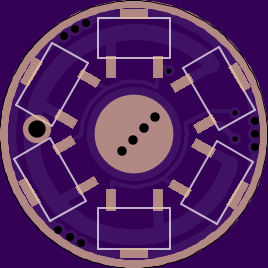
I’ve continued to barge forward with the existing configuration (1+2+3+FET with PWM on 1 & the FET). Clearly there has been a minor overhaul to the layout. Here is what it achieves:
- All small components have been labeled, correctly I hope. D1 just got a little triangle

- All non-GND pads are a minimum of 1mm away from the outside edge!
- All physical component outlines are a minimum of 1mm away from the outside edge!
- Zener footprint added. (optional)
Note that there is interference between outlines and bare copper, so finished boards may look different.
https://oshpark.com/shared_projects/coO0VDbI

Wight, it looks like you’re not using a GND poly but instead trying to trace out GND airwires?
It’s a better practice to skip over ALL GND airwires, just draw a big poly around everything and let eagle take care of it all as the final step. This also eliminates you having to manually put a GND ring in copper (just draw it in tstop). I do notice you have a couple poly’s already on the board (atleast I hope those shape’s are poly’s and not just a bunch of lines drawn together), you’ll need to assign them a lower rank (higher number) so your GND poly can be ranked as top priority (number 1).
If this doesn’t make sense let me know and I’ll shoot you over a sample .brd to look at. It also makes the boards just look better in general. Don’t forget to turn off thermal’s on the top, you don’t want them on the FET’s GND.
I stopped doing that for some reason. Can’t remember why though. The pours you see are poly’s.
Now that you’ve brought it up I’ll take another look a it on the next edit. Thanks for mentioning it.
I think that for my workflow leaving GND traces for the last step is a definite no-no. OTOH I might start using a GND poly to wrap a completed driver up in a nice looking way. The problem remains that any major refactor of the driver would require removing the poly and droping a bunch of GND traces again so that I can think correctly. It’s easier for me to paint myself into a corner when I’ve got a lot of airwires…
I had this issue too at first but I’ve actually found it easier to do not tracing them now that I’m use to it. To make major edits you can save, close the board then reopen and the poly wont be filled in so you can see to work / reroute other traces, hit ratsnext and boom, its all back and conforms to your newly added / rerouted traces.
Here’s a great tutorial on using poly’s (mostly for GND fills but useful for all poly’s)
http://dangerousprototypes.com/2012/07/18/eagle-polygons/
I dont want to say Matt’s way of doing things is wrong, first it obviously works well enough for literally thousands of lights running BLF drivers and secondly him and his video’s are directly responsible for a lot of us being able to use eagle in the first place but I really wish his video’s would of shown this, its a much better practice in general to handle all the GND’s both for basic design / board layout and for how stuff runs once assembled.
Also one of my biggest pet-peves was when the GND ring trace would pull off the edge of the board, pretty much impossible with a poly.
Nao entendi nada do que voce falou…
You’re certainly correct about the strength issue. On the bench I’ve torn off several thin GND rings while doing testing. Using a pour instead can do nothing but help.
I like the idea of lots of gnd ring vias to anchor the copper, also on critical led+/- pads. I like having some of the gnd ring vias a bit larger in dia to allow for ground wires in stacked boards or odd installations.
How far is the progress in terms of firmware?
Did you use Starfirmware as base? The Clicky or the momentary Version?
I would like to use this for my Y3 and Courui.
I have not fully investigated the newest STAR Firmware but it looks like if it would work out of the box for moon with 7135 and other modes with FET. I just need to add a if construct to toggle the 7135 pins in the right mode…
[turns to face RMM with fingers interlaced and an expectant smile on his face]
“So Richard, when can we expect kits for sale on MTN?”