Can someone please unscrew driver board and tell me what is the marking on IC6 chip? It is just 4 screws and you made my day ![]()
Thanks, Mike
Hmm, I looked at your pic over on CPF:
- I think IC6 might be AO3415 based on the topmarks. Alpha & Omega Semiconductor
- It appears that you have the TK35UE (it has an MT-G2). This could be an important point when you are asking for help, the UE does not necessarily use the same driver as other TK35 models.
- Would you mind posting pictures of all parts of the driver (including the top PCB)? Thanks!
I have old TK35 with replaced battery carrier and driver - old was broken, so they send me new one. Picture is just found on the net. Part on mine driver board become ashes. I will make a picture of my tk35 tomorrow.
Mike
Gotcha, sounds like a plan!
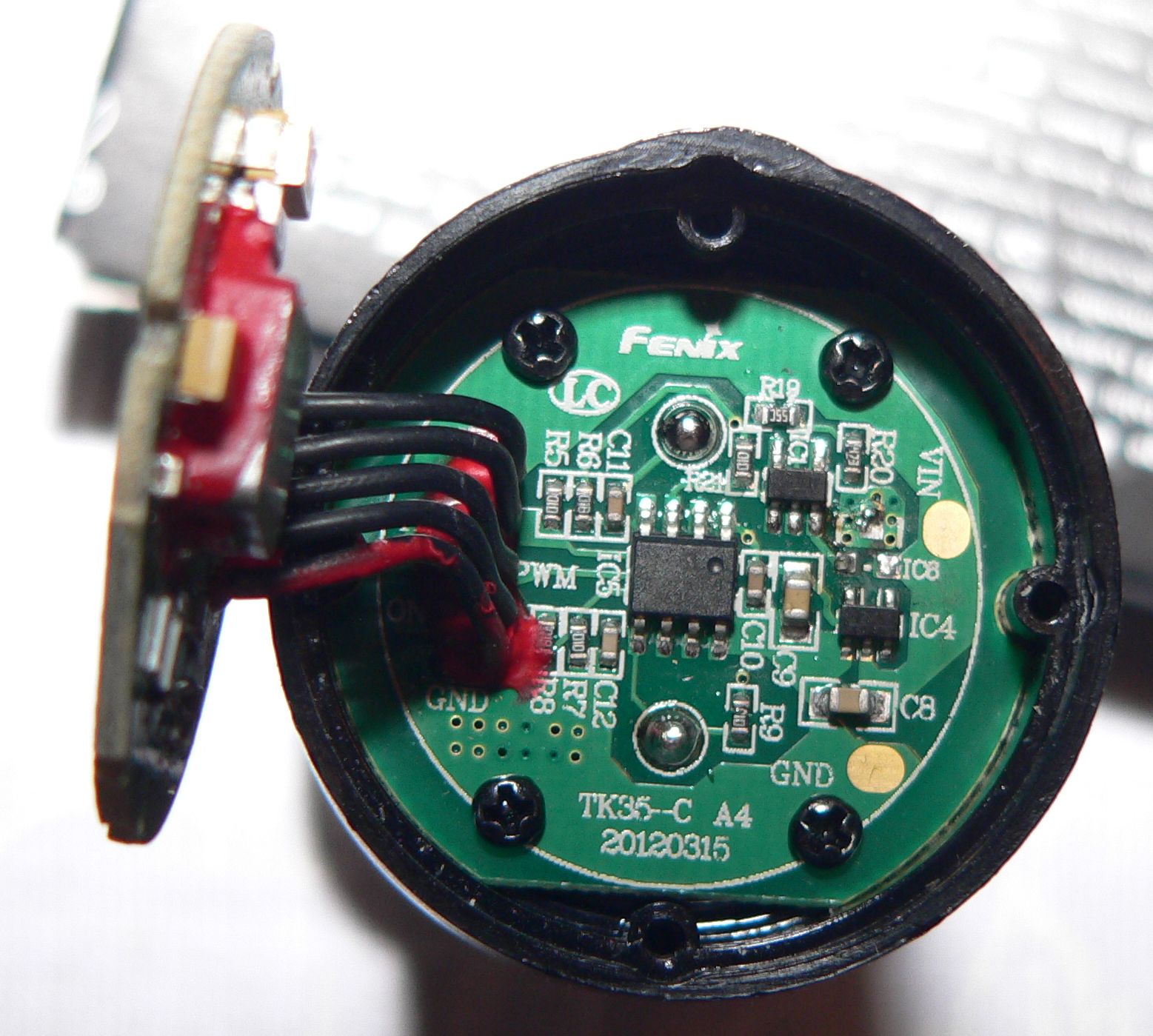
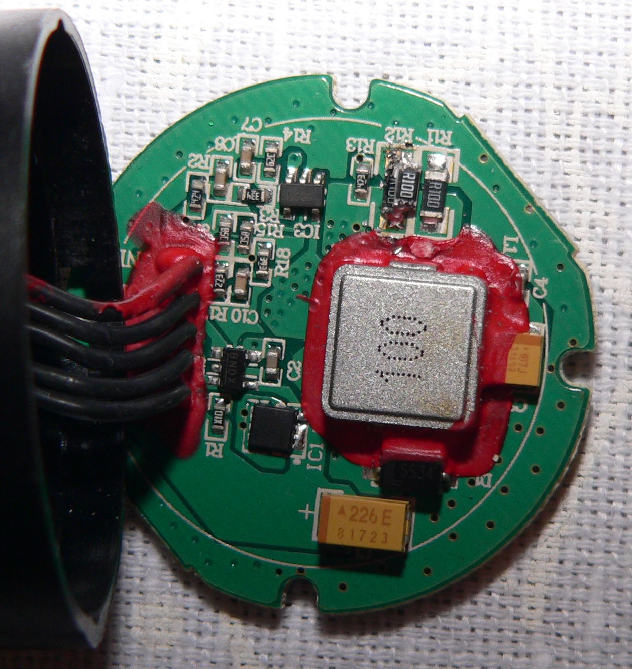
My driver boards.
Mike
Thanks for posting the pictures.
I didn’t learn anything new that pertains to your blown up IC. I do still think that it’s likely to be AO3415, fortunately they are cheap and readily available.
One more picture found on the web:
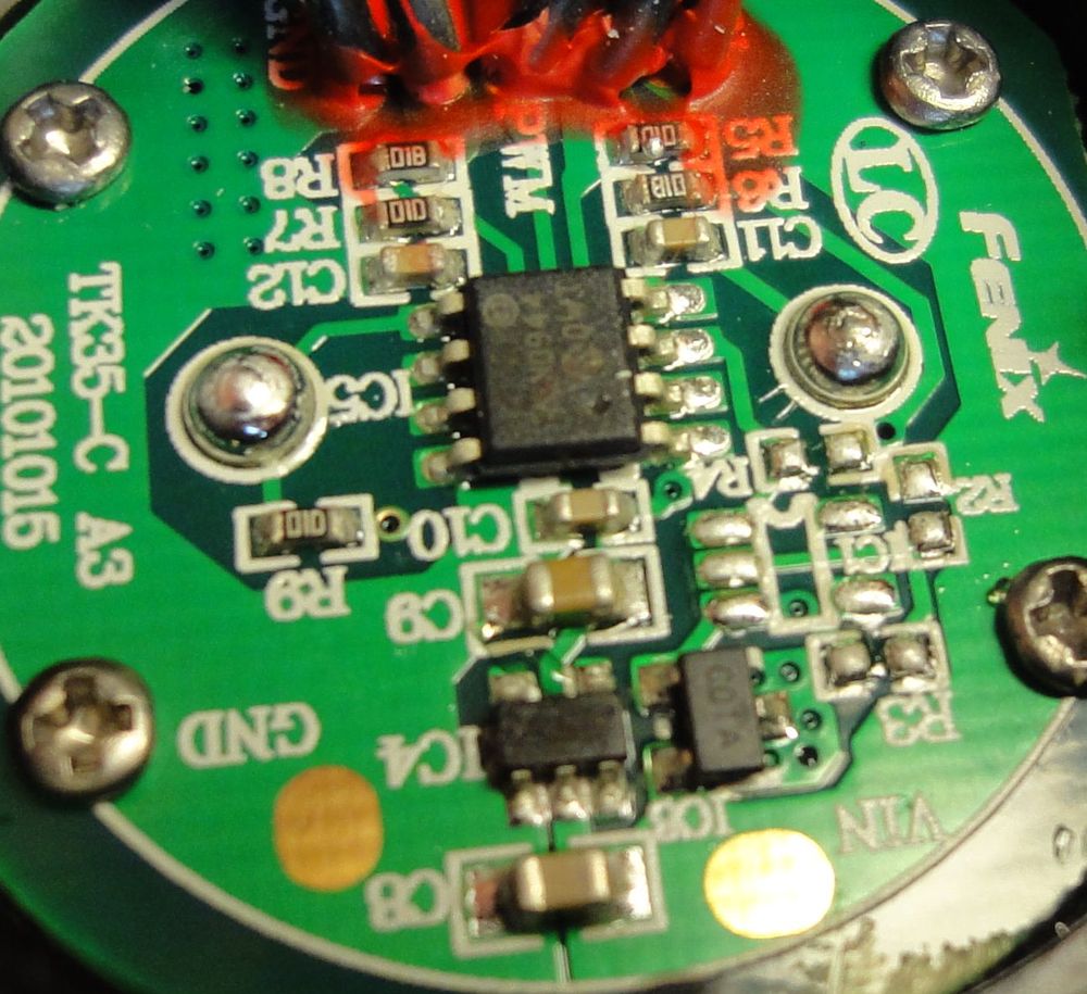
Differet layout. There is C01A. What it can be?
Mike
I do not recognize the markings on that one. There are many P-channel MOSFETs on the market. I think it’s safe to assume that it’s just an equivalent one to the AO model.
Sp5it, one leg has a trace which goes to IC1. I see from the new picture that the trace also connects to a via. Does the via go to BAT+ like the other group of vias? Or what?
I see on the latest picture you found IC1 and the three resistors around it are all unpopulated.
Source goes to + of driver board
Gate to other IC on PCB.
Drain to Batt+
Mike
Please look more closely at the picture in post #6. Gate does not go to an IC. Gate goes to a via. [IC1 is unpopulated!]
Look at post #4 - driver board from my torch. Burned IC6 already removed.
Tomorrow I’m going to buy p-mosfet, we’ll see if it gonna work.
Mike
I’ve seen you post #4. I understand what you said. I understand the picture.
Please closely compare the two drivers. Your driver has SIGNIFICANTLY MORE COMPONENTS installed on the PCB. One of those components, IC1, is blocking your view of a via.
Please note that in the picture from fonarevka.ru, the IC1 position is not populated (not used). Instead only the via is attached to GATE on the FET which burned on your driver.
Torch repaired. Thanks to Wight. It was p-channel mosfet. I put 4.2A 20V.
Thanks, Mike
That’s good! I’m still curious about the answer to my question from above. It would be nice if you got a chance to check where the gate trace actually goes to (after it goes through that via under IC1).
Nice work guys.