RIP, DP. You fought the good fight and and went down swinging. Can I help you resurrect it by purchasing 2 sets of boards/parts or did the wife file a DNR?

Hahaha!
Maybe posting some sort of testing protocol with standards for sense resistors and the results for each. This will give us a starting point so we can plot various drive currents vs input voltage in a larger sample size.
Earlier I edited the STAR on-time firmware for Mattaus / DBCstm to use with 150Hz PWM. I’m no longer certain that we need the low-speed PWM, but it’s not hurting anything. I posted both the .hex file and the source code. The firmwares that I have modified so far are both flawed in some small way – the first one has low voltage protection disabled (a good thing until we finalize the sense resistor values) but has a really annoying on-time no-memory configuration. The second has the same annoying config and has a ballparked 2sLVP setup for the values that Mattaus wrote about in an edit to the OP. I will compile a new firmware that has normal on-time memory, LVP disabled, and 150hz soon. Later we will confirm whether we need 150Hz and we will determine the proper setup for LVP. See these posts for details on the firmwares and download links: #209 & #226
Double check with DBCstm (I will edit this once he confirms) but as I’ve mentioned previously, in order to disable LVP leave R2 and R3 empty AND short pin 7 & 8 on the MCU. Do not populate R2 and R3, we do not have a working LVP with these firmwares. If you have trouble with LVP kicking in anyway, short pins 7 & 8 on the MCU.
In post #99 Mattaus talks about testing your basic build. Here is what’s relevant to us at this stage:
- It’s possible to test only the buck circuit without PWM, modes, etc. See steps 1-4 in Mattaus’s post for details on that.
- We know the voltage regulator works, if you assemble that properly there’s no need to test, see Mattaus’s post for instructions if you think you’ve screwed up.
In order to control drive currents, use
This means:
| Resistor (Ohms) | Output (Amps) | Approximate resistor stacking |
| 0.025 | 4 | Stack 0.1, 0.1, 0.1, and 0.1 |
| 0.033 | 3.03030303 | Stack 0.1, 0.1, and 0.1 |
| 0.04 | 2.5 | Stack 0.1, 0.1, and 0.2 |
| 0.05 | 2 | Stack 0.1 and 0.1 |
| 0.066 | 1.515151515 | Stack 0.1 and 0.2 |
| 0.1 | 1 | |
| 0.2 | 0.5 |
In order to know losses through the driver we must know efficiency. The measurements should be as close to simultaneous as possible. In order to do efficiency calculation we need to take the readings in the table below while under load. The driver must be in high mode or without the MCU present at all. We do NOT need to know those figures for medium, low, or moonlight right now. That will come later.
| current draw at the battery (amps) |
| voltage at the battery (volts) |
| current to the emitter (amps) |
| voltage at the emitter (volts) |
For now it would be good to gather those figures in these scenarios:
- Different vOUT (XM-L, XM-L2, MT-G2 all have pretty different Vf ranges.).
- Different drive currents (not modes). Use the sense resistor table I posted above and be sure to specify whether you used a stack (less accurate), a 5% sense resistor, or a 1% sense resistor (most accurate).
Thanks wight, I’m placing an order for some other parts and will include those test values in .1%.
The Knucklehead ran my MT-G2 just fine with the LVP resistors absent, and pin 7 bridged to pin 8 on the MCU. I didn’t get to do thorough checking as I accidentally killed the regulator soldering the ground ring to the heat sink.
The board, with the modified firmware as described above, is and has been working fine with the MT-G2 with pins 7 and 8 NOT connected, but no LVP resistors.
I have slept since doing all that, so am now clueless as to what is going on with my Knucklehead. Sorry.
I just looked at it closely, there are no LVP resistors, pins 7 and 8 are clear, and the driver works with 2 cells to drive the big emitter. This is still the way it was set up when I was running it for longer than I’ve ever run an MT-G2. And there is no memory, start in lo each time.
Still no word from OSHPark on the new boards shipping. Everything else is on hand.
Thanks DBCstm, I’ve edited my post accordingly. Like I said, I’ll do another quick edit as soon as I get a chance and post a firmware with regular on-time memory, the same modes (I guess?), and no LVP enabled. That way there won’t be anything to worry about with the floating ADC pin (pin 7).
Same thing for me, waiting on boards.
Were your boards a snug fit in 17mm driver holes?
I’ve been revising the layout. I got a notification today that Oshpark has sent these test boards to the fab:


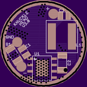
The only area of the board not covered in traces or copper pours is some of the area underneath the inductor. Thermal vias have been added wherever practical, electrical vias have been minimized. I think there is now one via for the PWM signal, one via for VINA (to BAT+ currently), 1 via for VINSW (the big one; BAT+ again), and the vias in the corner between the MCU and the PSU section double to connect the ground plane there to the rest of the ground plane. So a total of 4 electrical vias, the rest are all there to connect the copper pours thermally for the LED2001’s benefit.
Question - how have you forced solder-mark to be applied over the vias? On all my boards, wherever there is a via there is a ring of exposed copper around it (see OP for examples). For the most part this is fine but I'd be interested to know how you can pack in a sh*t-tonne of vias but still have nice angular component footprints.
In Eagle you go to Edit~~DRC and open the Masks tab. Adjust the “Limit” value to a large size. When you add new vias which are smaller than this size they will not have anything added to the tstop/bstop/etc layer, so mask will be applied. I think that changing the Limit value may not effect all pre-existing vias, or at least not consistently. EDIT: or it could just be drawing glitches in Eagle~~ I run into those sometimes.
If you need to override this setting for a single via you can. You must open it’s Properties and check the checkbox for Stop. Of course when it’s already sitting in a pad for another thing there is already a nice rectangle in the appropriate stop layer - so no change needed.
Sweet. Learn something new every day. Thanks.
This board was already going to be more difficult to solder on due to all the thermal vias and the tighter layout. I figured tented vias would be important to help stuff self-align during the reflow. C2 is one of the tricky ones - I think it may still want to act funny due to the big via.
I have a little bit concerned about the A ground is not connected to P ground at one point.
Looks like you got termites ![]()
Man look at all that open space…but that is what is needed to wick all that heat away I suppose
And reading your tutorial on the vias, nice on how to reduce the stop size, make it an electrically conductive “hole” rather than a solder pad…excellent!
The A ground is connected to the P ground.
GND / PGND / Exposed pad (pins 4, 8, and 9) are all connected together on the original v3.0 board as well as the one I just posted.
Are you saying that they should not be connected so close together? I could disconnect the PGND pin from the main copper pour (the one the exposed pad is part of) and then route a thick trace under the inductor to the right-hand side of C3. That would make it more like the application circuit in the datasheet. What do you think?
Yes, try to layout as the datasheet. The ground of Cin (C2), Cout (C3) and P ground of the LED2K1 should be an individual group and then connected to the A ground. This arrangement will avoid the high current noise signals mixed into the analog section of the IC.
wight is there no ground ring on the battery side of the board?
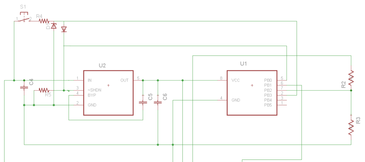
Yes, but why are PB3 and PB0 of the ATtiny parrallel?
Also I do not know if the voltage you get through R4 will be enough to pull PB3 to high when the switch is pressen.
Especially when using different battery setups.
As far as I understood the datasheet it always drains about 1.5mA.
The VINA is for analog dimming. Since there is still a lot of space on the board perhaps it is possible to add a low pass filter for the ATtiny and additional to PWM dimming get analog dimming.
That would get us a lower low (5% is not that low…) and would be more efficient.
Regards
OK, thank you. I will attempt a revision to address this. Do you think that noise from the layout could have caused the LED2001 failures more than the high power dissipation?
^Thanks!
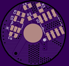
Oops? There is no exposed ground ring. Of course almost the entire battery side is ground, but it’s all covered in purple resist. The large areas of light purple (drawn with horizontal lines through them) are solid copper covered in resist, called “copper pours”.
They are parallel because one pin must be set as an output in order to hold the SHDN pin on the LT1761 high. We still want to know about button presses though, so we need to use another pin to read those. If we just used one pin we would have to set it to output and make it go high, we would be unable to do input at the same time. I made a mistake in my schematic though! When we use the output pin on the ATtiny to pull the SHDN pin high we must also use a diode to prevent it from pulling the input pin on the ATtiny high when the switch is not pressed. Oops. Please see below for a schematic I revised in MSPAINT just now. I added a diode to prevent PB0 (output) from pulling PB3 (input) high.
One of us is misunderstanding the datasheet (could be me). My understanding is that the LED2001 does not have analog dimming. I suspect you are misunderstanding the purpose of that pin. Here is my understanding: VINSW serves only the internal FET. VINA serves the rest of the LED2001’s functions including analog comparators & etc. Please review figure 3 in section 5 of the datasheet and let me know if you think I’m misunderstanding this thing. If my understanding is correct, I kind of doubt that the FET has a 1.5mA parasitic drain on it’s own - so that drain is probably from the rest of the chip (VINA). Disconnecting VINA should prevent that drain… maybe!
…can the text denoting Knucklehead v3.0 be moved to the battery side of the board so it will be seen when installed in a light?
I just haven’t done much with the text yet because I was focused on the other aspects and Mattaus’s personal logo got messed up anyway (by me). Since I’d mangled it I just deleted it and left it off because I figured it needed to be re-imported to fix the problem he was showing you guys earlier (it didn’t look like it should).
If the momentary stuff Fritz and I have been discussing works out there will be another fairly major board revision for that, plus any changes to satisfy the noise reduction needs Microa brought up.
All that “empty” space on the bottom looks like a perfect billboard to me ![]() EDIT: well, other than the area covered in vias. It’s tricky to put text in that area…
EDIT: well, other than the area covered in vias. It’s tricky to put text in that area…
Well, since there’s so much space available, could we make it read like a billboard? Saying somthing like “Don’t Mess With This Area You Knucklehead!” so when people take the battery tube off the light it would become immediately apparent that they should stop! ![]() lol
lol
Needs a BLF on there too ![]()
