Nichia E17A/E21A series (April 19th: updated with output tests in the OP)

New from Nichia, flat leds no bigger than the die, E17A is 1.7x1.7mm, E21A is 2.1x2.1mm. The E21A is rated for up to 1400mA continuously/2000 mA peak. The thermal resistance seems unrealistically low: 0.3 deg/W for the E21A. Claim is 'highest flux density in the industry', sounds like what we want to hear :-) Big drawback for us flashoholics: a two-pad solder lay-out, no thermal pad. But I can see 4 E21A leds soldered to a XM-Noctigon happening, or even better, four E17A's soldered to a XP-Noctigon. My conclusion sofar: great leds, but perhaps not for the majority of us, requires some skills, but then...

Update April 19th:
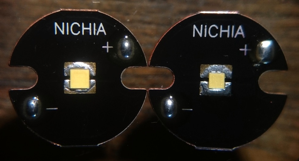
I tested two of these, one E17A 5000K 80+CRI (NCSWE17AT) and one E21A 5000K 80+CRI (NVSWE21AT) for output and voltage. Because these leds have the two-pad solder lay-out, I tested them on the only suitable boards available to me that can be easily used in flashlights: my own 119-boards that I had made by Kerui electronics: 1mm thick copper core, non-DTP, the solder-pads widening into a large pour under the solder mask (see my signature line for a thread on these boards).

Here is a size comparison to other well-known leds without dome: left the E17A, middle top a Cree XP-L HI, middle bottom a dedomed XP-G2, right the E21A.
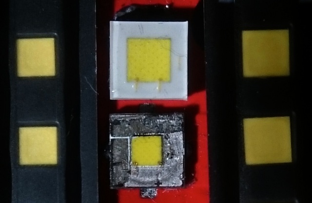
It looks like the E21A has a similar die size as a XP-L Hi, and the E17A is slightly larger than a dedomed XP-G2, but if you have a look (picture below, at 0.5mA current) at the light emitting area of the E17A (the E21A shows a similar picture) you will see that despite the looks the led is not a bare die, the actual die is considerably smaller than the total led surface, while the two shown Cree dies are evenly bright up to the edge.
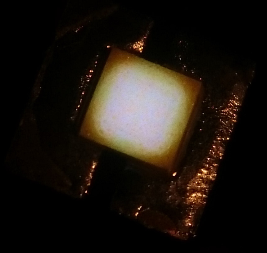
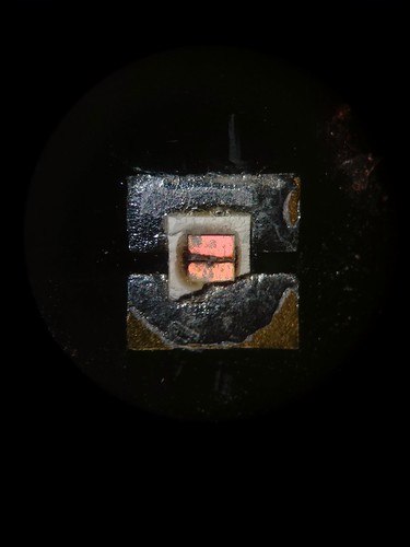
So the emitting area of the E17A is similar or even a bit smaller than a dedomed XP-G2. So at equal output the E17A will have better throw. Here is the led after the test with the phosfor scraped off, the actual die is about 1mm x 1mm (and badly damaged and cracked in the middle from the test )

Let's move further to the output tests.
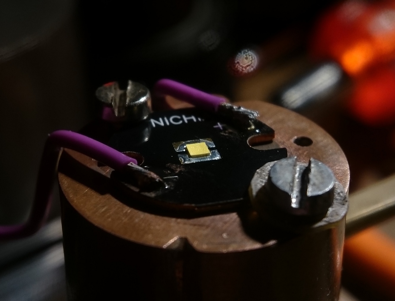
The output test was done like all my more recent emitter tests. I described it in detail in my XP-L test. , with two minor differences that should not matter significantly for the results: I used my Integrating sphere no. II instead of no. I, and for the current I used a clamp meter, which appears to measure 0.1A lower than the power supply current-reading that I used before.

In summary: 1) just one led was tested of each type, reflowed on my non-DTP copper board 2) I used my large version II integrating sphere with high quality luxmeter, 3) the output numbers and voltages were measured with the led close to 'steady state' for each current, so warmed up and settled, you should be able to get these numbers in a well heatsinked flashlight. Mind that these are output numbers of the bare led, in a flashlight there will be losses from light obstructions, lens and optic, 4) output is in 'djozz-lumen' defined as 1/550 of the output of my Sunwayman D40A on high setting, which I hope is close to the real lumen, but at least is consistent over all my emitter tests done in integrating spheres.

The newly obained output data were plotted together with earlier obtained data from a Nichia 219C 5000K 80+CRI, and a Cree XP-G2 S4 2B, for comparison. The E17A was tested up to where it burned to death (4.6A), the E21A led was tested up to 5A at which point it was not burned yet. Later I found the death current to be around 7A.
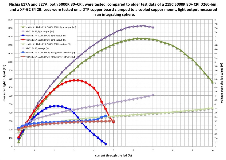
What can be seen:

*at least on these boards these new leds can handle way less current than the 219C of XP-G2. And actually I expect them not to behave much different on a board with better heatsinking like Clemence's upcoming VirEnce boards. That is because my boards with the Nichia 144A leds have proven to handle way more power than in these tests without problem.

*the voltage is nice low, at moderate currents slightly higher than the 219C

*the output and efficiency up to 1A is good, the E21A is on par with the 219C and XP-G2

*I would use the E17A up to 1A, and the E21A up to 2A. This is actually according to the datasheets for these leds, it seems that they can not be overdriven like many other leds.

When these leds finally blow, way above the current with maximum output, it is clear where it goes wrong: in the gap between the solder pads:
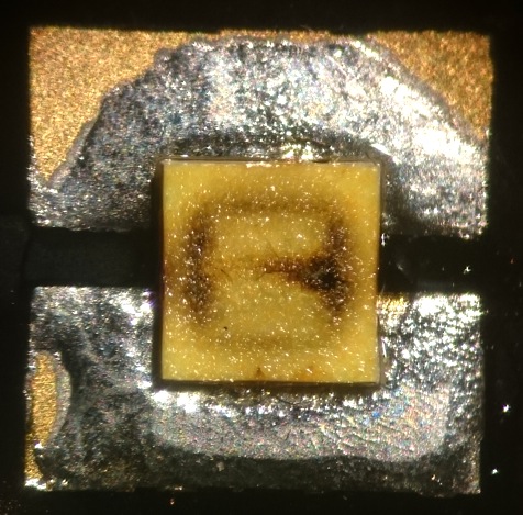
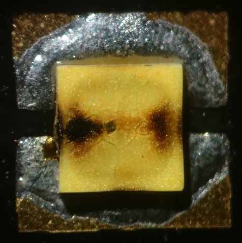
But at reasonable current with close to highest output, I don't think that a bad heat path from the led area above the gap has much influence on the output of the led. I think.

Conclusion.

So these leds are are not:

*great high current high output leds that can compete with high output leds that are around already

*the new throw kings: the dies are small indeed, and they are dome-less, but they lack the output density of dedomed Cree leds and Oslon Black Flat.

But I can see a use for these leds in small lights with moderate current, say AA-lights with a boost driver. I have not tested the beam that they produce but I expect it to be very good. And being Nichia's these leds will be available (through Clemence) in very good tints and CRI, I understand even in R9080 quality.

Thanks for reading!

This looks like fun.

I want one! Who needs a separate thermal pad? If Nichia believes it don’t need it, or there is no benefit to it, who are we to say otherwise? So, when does the GB start?

Edit: Luminous Flux of the E21A @700mA roughly compares to XP-G2 S3 or XM-L2 T6. Package size is 2.1mm x 2.1mm for the Nichia, 3.45mm x 3.45mm for XP-G2 and 5.0mm x 5.0mm for XM-L2. So, did I say I want one? Maybe I want a few dozen! O:-)

These new Nichias look very promising for tiny pocket throwers.
How is the color rendering of these pipsqueaks?

Looks like they come in two flavors - 70CRI and 80CRI

Thanks for finding out the flux comparisons!

The package comparison is not really fair, for flux density (which is the relevant factor for throw) you need to compare die size: the XP-G2 die size is 1.5x1.5mm, compared to 2.1x2.1mm for the E21A. That suggests that the XP-G2 still wins, even though Nichia claims that high flux density. But what will happen at high current on a copper board is the question…

Since there isn’t a separate thermal pad, I don’t think a copper board will have any advantage over an aluminum board. Since the heat transfer will be going through one, or both, (I’m assuming it will be the cathode) contact pads, there will be a dielectric layer the heat will have to go through.
Sure, you could shift the emitter so part of the cathode is making contact with the DTP, but then you will be dealing with permanent direct drive.

Yeah, I knew that, but I couldn’t find anywhere that says what the die size is. If you can link a source for me, that’d be great! And of course, the XP-G2 definitely wins by a long shot, because that wasn’t even the highest binned XP-G2! :wink:

Although for flux density, only the die size counts, package size does matter in other ways. I’d still like to play around with some of these Nichias. Really, if you think about it, it would seem that Cree and Nichia had some similar advances. Cree starts making flat emitter packages from existing high output dies, and also squeezing dies onto smaller packages. Then, Nichia combines those two in a “chip IS the package” deal with a flat profile. If Cree wanted to, they could easily make a direct competitor to the Nichia E17A and E21A series. They’re already really close with the packaging, and way ahead in flux density!

A copper board should still give a little advantage, because it is copper. I agree that DTP isn’t even a consideration, but copper should do better than aluminum anyway, I’d expect.

If you mount four E17A leds on a XP-Noctigon, you can have all the plus-sides of the leds on the DTP-pad and thus the flashlight body, the led-minus’s will be on the two ledwire-pads combined. Then use a reversed battery and direct the minus of the battery to the ground of your driver, making sure that the led-side ground ring of the driver does not touch the body, while the batt+ pad does make contact with the body. You can rebuild the driver for this by isolating the led-side ground ring of the driver with Kapton-tape, and boring out (just slightly, from the battery side of the driver) all the via’s going to the other side to make them loose all contact to the other side, then make two holes and wire the old batt+pad to the led-side ground ring, and the old batt-minus pad to the led-side+. Are we still there? ;)

I guess I should assume you were thinking about this.

Umm, I don’t know much about drivers, but would there be a way you could re-work the driver to interrupt power to the LED+ instead of the LED- so that none of that drillin’ and choppin’ are necessary? Or is driver design such that your drillin’ and choppin’ IS the easy way? Or is it that the components all work on the negative side, so switching positive is basically impossible?

Good gosh man…so you’re basically saying that we could all be running around with 12 emitter Convoy S2+s on a triple XP board?

Uhm, I guess so… :sunglasses:

Say you can overdrive the E17A to 1500mA on a XP-Noctigon, the output (extrapolated from the Nichia datasheet graph) could be 560 lumen, times 12 is 6720 lumen, with losses 5000 lumen out the front.

… for a brief moment because you are running your S2+ at 18 amps/63W O:-)

w00t!
…and there goes the battery tube - melting away… }:slight_smile:

Thanks for showing off these LED’s Djozz. I can think of a couple fancy ways to design a special star for this led.

One approach is to use a dielectric PVD coating to electrically isolate the star from the rest of the light while retaining optimal thermal transfer. Imagine a two piece star, split down the center, with the dielectric PVD coating on the bottom and sides of the stars semicircle halves. Butt these together. The gap at the center would be practically non existent but it could be shimmed ~.001” or more and that gap filled with high temp thermal epoxy. The gap between the halves would widen and bevel after it left the area under the LED, taking on more thermal epoxy to more strongly keep the star together as one piece.

A less elegant method would be to take an aluminum disc (or the head of a light) and machine two pockets across it, with only a .002” wide divider in the center between them. Anodize the aluminum, then embed a thick, machined copper strip into each of the pockets. A small amount of high temperature thermal epoxy would be necessary under the copper strips. Or, omitting the.002” aluminum divider, (so one contiguous pocket) the copper strips could be shimmed in the middle when “set” into the pockets. Filling the shim gap would be high temp epoxy. The gap could be made ~.001” or wider with this method.

Interesting. Very nice find, djozz!

Hoop, that makes me think of a board I made for a Luxeon Z once: LuxeonZ, the making of a copper board, and testing
It still works but upon heating up, after a few minutes something deforms and shorts, when cooled down it works again. I think I made the AAA insulating layer too thin.

You could use the DTP pad for probably the cathode, and use enough thermal compound between the star and pill that there is no electrical pathway. It’s not ideal, but better than permanent DD, with a little better thermal characteristics.

It would be nice is someone made a cooper MCPCB with its footprint and a thin or heat conducting insulation layer. The Cree LEDs must have an insulating layer in them, but apparently it conducts heat better than the insulating layers of existing MCPCBs do.