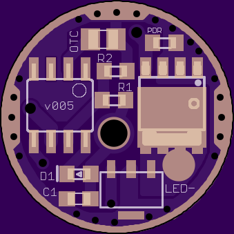
This board is really dense populated! you made a great job!
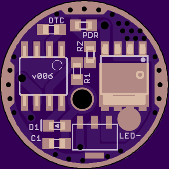
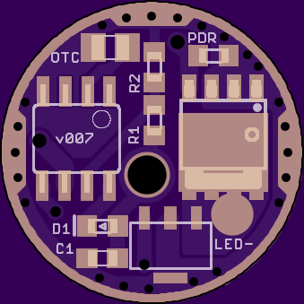
I have already changed OTC pads size to 0805, i have had to remove some vias, and voltage resistors may not be easy accesible, placed that way between tall components, but i think it is done.
Your board is clearly improving, but here are a few things (in no particular order):
Your silk lines are way too thin to be produced as specified. OSH Park or the fab will automatically thicken them for you, but I prefer to thicken them myself (for full control). The worst offender is the marking “PDR” - I suspect that this may not be legible after thickening. I don’t remember how thin OSH Park goes and I can’t find it on the specs page right now: OSH Park Docs ~ Services ~ 2 Layer Prototype Service Maybe someone else can help. Maybe I normally use approximately 6mil minimum? I’m not certain at the moment.
I still don’t think that the board is setup well for a Zener mod. If you’re still not clear on the Zener circuit maybe someone will throw up a quick diagram at some point. Clearly Zener compatibility is not required - it’s just something to think about.
R2 looks suspiciously close to the MCU for a stock programming clip to fit. R1 is definitely OK, the clip doesn’t extend into that area.
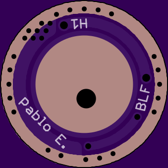
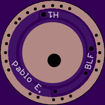
Version numbering seemed to stop at v5 where the the driver’s “H1” designation just started getting extra letters added to it? I suppose that’s related to the bypass hole.
Thank you too! it is improving thanks to all of your help.
I going to reply in the same order:
I didn’t know, i’ve took a look at a v003 I ordered to see how things were goin, and yes, silkscreen lines are thickened, but there is no small markings to check legibility :-/
Darn! i thought i got it, thanks for pointing it out.
Sure it is not a mandatary, i will see what i can do, but if it is not done like i thought, i am affraid it wont be possible.
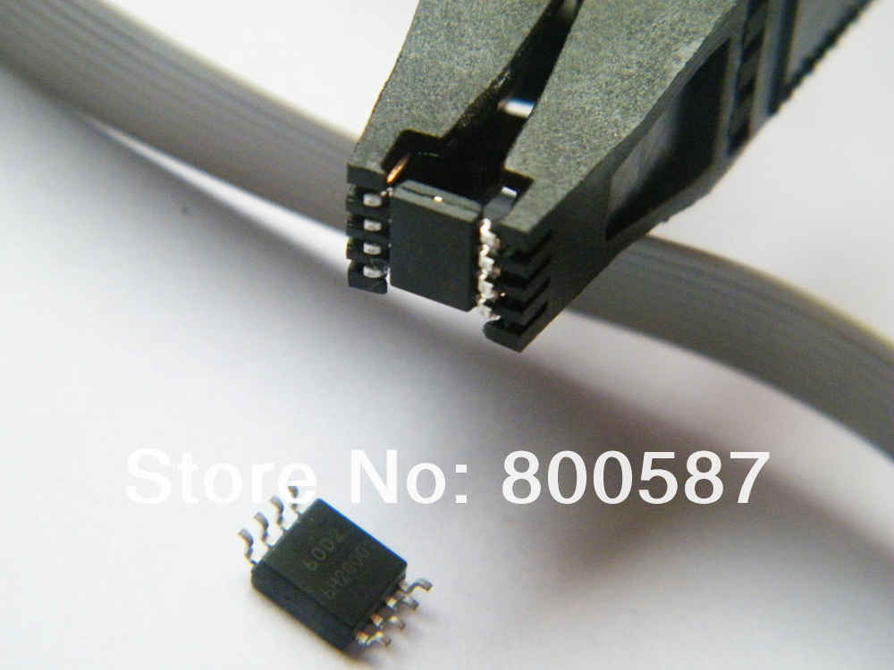
Well, my clip is not wider than MCU, but now i see the other clip version on google, seems that it could suffer this problem.
Yes, it is related to the bypass hole and the bigger cap.
I have no clear how to mark them, as a new version or as a different branches.
I dont want people to think newer boards are better, when they are only different, but i am not happy neither with the extra letters, i think i am going to back to numbers as it keep things simpler.
Is a chinese no branded one you can find on ebay, aliexpress and many other sites.
I got it from this seller: Henny Liu’s store , but i don’t recommend him/her as i got different clip from which is shown on advert images, so random version could be sent.
I need some help. So far everything I’ve done has had a perfectly circular milling layer. How do I do other shapes accurately? Like an SRK driver with the tabs, or a tailboard in the SRK “flower” shape or for a ZY-T08?
Easy for you to say Richard! But this comes from a guy that build a D01 contact board and could not make a basic FET driver fit on board… I really suck at that program.
I just draw wires on the milling layer. If I need part of a circle I draw a full circle in the reference layer, than draw an arc in the milling layer and trace the part of the full circle in the reference layer that I want. I’ve never used the commands RMM suggests, I’ll have a look at them next time I need to do something like that.
Thanks DEL. The latest items I’ve ordered and just received thanks to this thread is the 15mm 7135 driver boards and the boards for momentary switches. Hopefully I can get a driver to work. :person_facepalming:
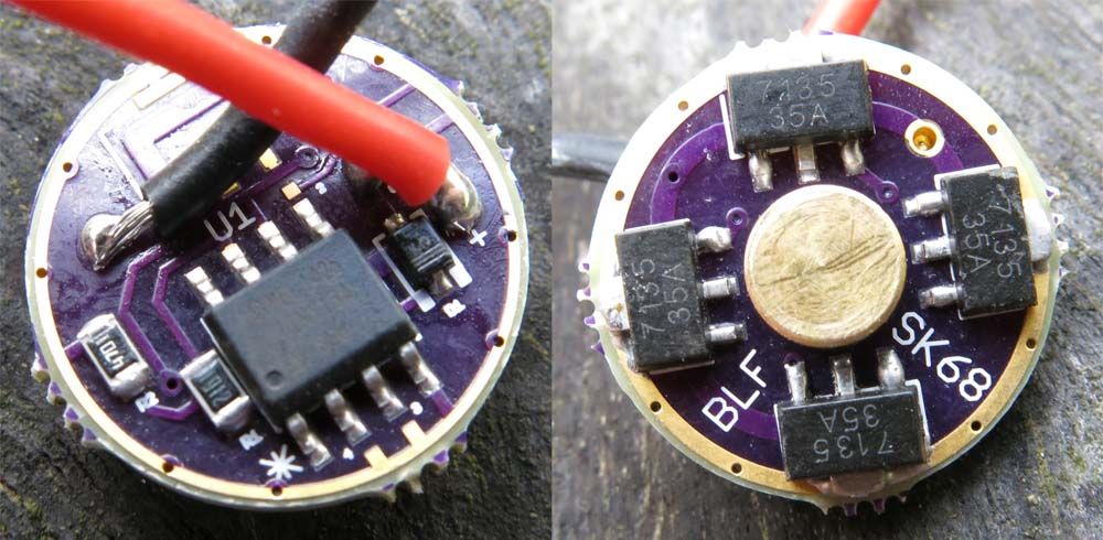
Wow. What a mission. Well for me it is anyway. I have just happily, after many failures over along period of time, managed to build my first working driver. Its the 15mm SK68 driver by WarHawk here.
I used an old 7135 driver for parts that never worked, flashed the MCU with TK’s Biscotti and we had light. To everyone involved, a big thanks. Yes there were lots of you here that has helped me over an extended period of time from soldering, flashing and answering many questions. YAA HOO.