[released] 17mm 8x7135 with Zener & dual-PWM + stubborn: A17PZL

Nanjg-105c replacement w/ added functionality. [Regular firmwares can be used by bridging pins 5&6 to make it work like a 105c or Qlite - new functionality requires flashing a current version of STAR or similar.]

Features:

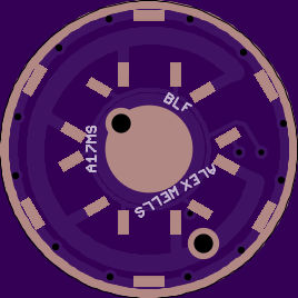
  • 1mm ‘tall’ component keepout around edge. While all plastic packages are 1mm+ away from the edge, 7135 tab is actually only 0.5mm away from the edge.
  • 7+1*7135 (so 8x) with dual-PWM, similar to RMM’s Moonlight Special (#1447) == identical functions, intended for use with the same firmware. Intended to achieve more efficient, consistent, and lower moonlight modes.
  • Zener ready. [SOD-123, our standard sized Zener]
  • Offtime ready.
  • Covered (scrapeable) PB4 (Pin3) input/output pad. Use for temp sensor or FET turbo w/ a stacked FET. The pad is ~1x2mm in size.
  • A significant arbitrary aesthetic design goal should be obvious… hint: it involves a lot of 0805s in a straight line!
  • Based on Cereal_killer’s post #44 in the DD+7135 thread I’ve used a larger GND ring on top where possible. The bottom remains 1mm. The exposed copper is 0.5mm on top and 0.25mm on the bottom with large ~1mm scallops.
  • Like some other recent drivers, this driver does have a reverse-polarity protection diode but bypasses the diode for the voltage divider. Due to this we are able to use any diode desired. Ideally we use a protection diode with as low a Vf as is reasonable.
  • The exposed spring pad is exactly 5mm, ignoring the via. The total copper under the spring is 6.4mm. [A signal trace is immediately outside this 6.4mm area, but everything should remain fully covered in resist out to approximately 7.4mm]
  • Both power vias are 1.3mm.
  • LED+/- pads are 2.6mm in diameter.

I established a very arbitrary design goal and stuck to my guns. All the 0805 components are perfectly lined up and spaced evenly from one another. Any differences in spacing are due to the low resolution render. Actual pads are significantly farther apart than they look. As far as the electrical design / schematic, this was directly inspired by the Moonlight Special driver. I’ve been discussing sequences of 7135s for a long time (and others were no doubt discussing it before I did). Under that system I’d normally put PWM on a single 7135 and then use toggles to turn on and off all the others in sets, typically organized something like (1, 1, 2, 4) or (1, 2, 3, 6) which allows the use of 1, 2, 3, 4, 5, 6, 7, or 8 IC’s at once (or 1 through 12 in the second set). At some point I came up with a hybrid driver which used an FET and all the other available outputs on an ATtiny13A in order to get as close to that ideal as possible + have FET turbo, but there are some downsides to that and more work to be done. Until RMM brought out the Moonlight Special driver it never occurred to me that there was any point to going less than “whole hog” on that concept. What RMM realized was that a single 7135 could maintain a very low, efficient, and reliable ‘low’ or ‘moonlight’ mode on one PWM output, and that if we hooked an additional PWM output up to another thing we could have both high and low current with PWM. (This driver is intended to use with either “full on” on all eight 7135s, PWM on all of the 7135s for all the regular modes, full on on a single 7135, or PWM on a single 7135 for the lowest mode.)

This driver has been cryptically named A17PZL, which can either stand for PWM, Zener, Linear… or PuzZLe.
:wink:

While the power vias are suitable for soldering your LED hookup wires into at a very large 1.3mm, there are also giant 2.6mm pads which are directly across from each other near the edges of the PCB. For many installs these probably make the most sense.


https://oshpark.com/shared_projects/dC3iqMxp


Additional pics in post #54.

Here is the original ‘work in progress’ OP. At the time the thread was titled:
“[WIP] 17mm 8x7135 with Zener & dual-PWM + stubborn”.

v008

I was concerned about the 3 vias located under the tab on the top 7135 which sits next to the Zener diode. I suspect that during reflow those vias could cause the 7135 to shift inwards and possibly bridge the Vdd/PWM pin onto the Zener’s pad. To combat this problem I distributed vias around the GND ring.

A178PZL?

= “puzzle” ? In order to taunt people when they realize that they should have soldered the MCU in place after the 0805 components?

pizzle? (wikipedia is your friend)

Yeah, puzzle. As in what order do I do this?

+1 for puzzle!

I’m for puzzle too.

Hah, I’m game. Puzzle sounds like a clear winner right now.

I updated the resist on the bottom to make reflow easier. There are now well-defined dams of resist between every 7135 tab and the exposed ring. The actual exposed ring is now very very thin, but the copper layer hasn’t changed (it’s 1mm) and I’ve added exposed scallops to make up for it.

Of course the silk is updated to reflect the name

It’s getting better all the tiiime. The scallops for the expander boards? It looks like there are some acute angles on the 7135 traces. What are the two lines across the L+ pad? They look like breaks in the copper leaving only two narrow paths for current.

EDIT: Thanks!

  • The scallops on the bottom are there to increase the solderable area which is available on the ring without scraping. Just something to make it easier to solder the driver into a pill in other words.
  • The only acute angles I see are where PWM traces “Y” together on the bottom. Is that what you are referring to? I did those on purpose because I like the way it looks. I do not expect it to affect operation or fab-ability. Are you looking there or somewhere else?
  • The lines across L+ are just an artifact of the OSH Park rendering technique and Eagle’s Polygon output. Polygons in Eagle are turned into a series of overlapping lines. This is normal and only affects the previews.

Aha! Yes the traces from the pwm pads to the ring and also led- to it’s ring but you know what you want. I’ve tried to minimize these by making the connector traces radial to the rings and connect to a pad corner but if it works wgaf?

Right. I think it’s about 6 of one and half a dozen of the other. Eagle doesn’t have dedicated tools for either task as far as I know. Neither way looks entirely natural. Aesthetics probably would have settled the question - if one looked better I’d have gone with that. Instead I settled on the one that was significantly easier for me to eyeball.

In a circuit like this, at these frequencies, as far as I know the only potential problem would be with a super, super bad fab not being able to produce something. Eg an “acid trap” problem, although I don’t have enough experience to know if that’s a real thing or just something people on the internet chat/whine about. I don’t think we’re going to run into any of that.

Looking good!

Thanks RMM!

It’s really a pity that Eagle does not have more features related to aesthetics, snapping, geometric layout, etc. CorelDraw would make short work of those revisions and make the result look better. Fortunately the final product is a tiny PCB, so my minor misalignments shouldn’t be super obvious.

In Post 10, the last pic you show, you left out the little circle that identifies pin one on the MCU.

I don’t like it.

I LOVE IT! :slight_smile:

Hahaha, and of course the text is rotated 180 degrees from the direction the MCU should face. Wow. (that was unintentional)

Updated to v012 -

  • Added a covered 1mm via for SW+ hookup from rear. Either pass your <1mm wire through and just solder onto OTC pad if you want or scrape before assembly and solder directly into the via.
  • Improved LED- trace on bottom in order to facilitate the chunk eaten up by the 1mm via that was added.
  • Increased LED+ and LED- vias to 1.3mm for cleaner and easier 20AWG/18AWG installation. Not really very important here, but I figured I’d do it for consistency. Maybe you’ve got a long run to the LED and want to use big hookup wires.
  • Updated silk slightly. Added orientation mark for MCU.
  • Updated GND pours for cleaner and more accurate look on renders. :slight_smile:

I think it’s ready for a release. I haven’t built one yet. I never ordered any because I wasn’t happy with the driver yet in earlier versions.


https://oshpark.com/shared_projects/BiFm1nwn