You can see the archived poll results on the Wayback Machine:
https://web.archive.org/web/20221220093741/https://budgetlightforum.com/t/-/72815
https://web.archive.org/web/20221220093741/https://budgetlightforum.com/t/-/72815
So I think final version of programming key and port I will use in the future designed
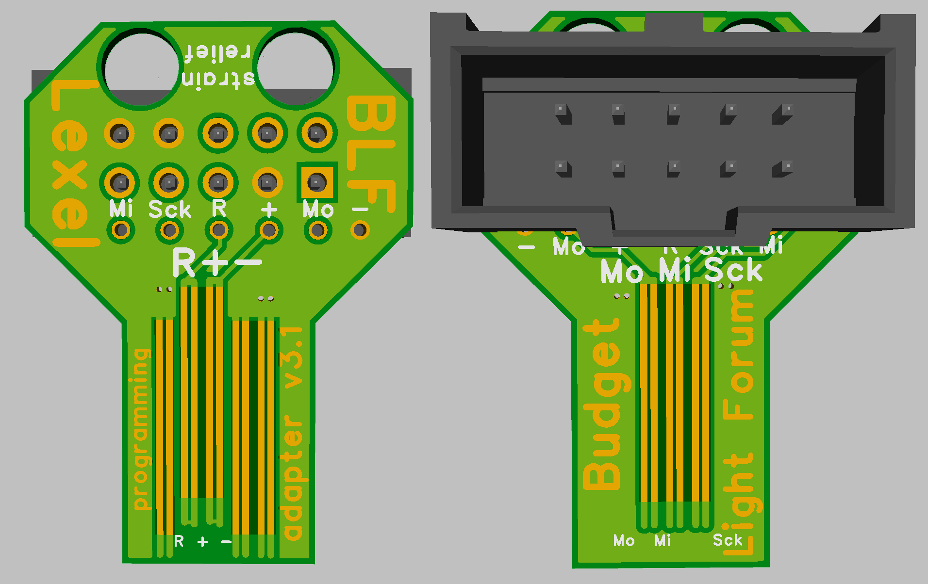
board thickness 0.8mm, small enough to even be applied to 17mm drivers
2 possible layout of the driver port, any combination of pads and vias is possible but at least 2 viases should be used for alignment
electrical improvements so far
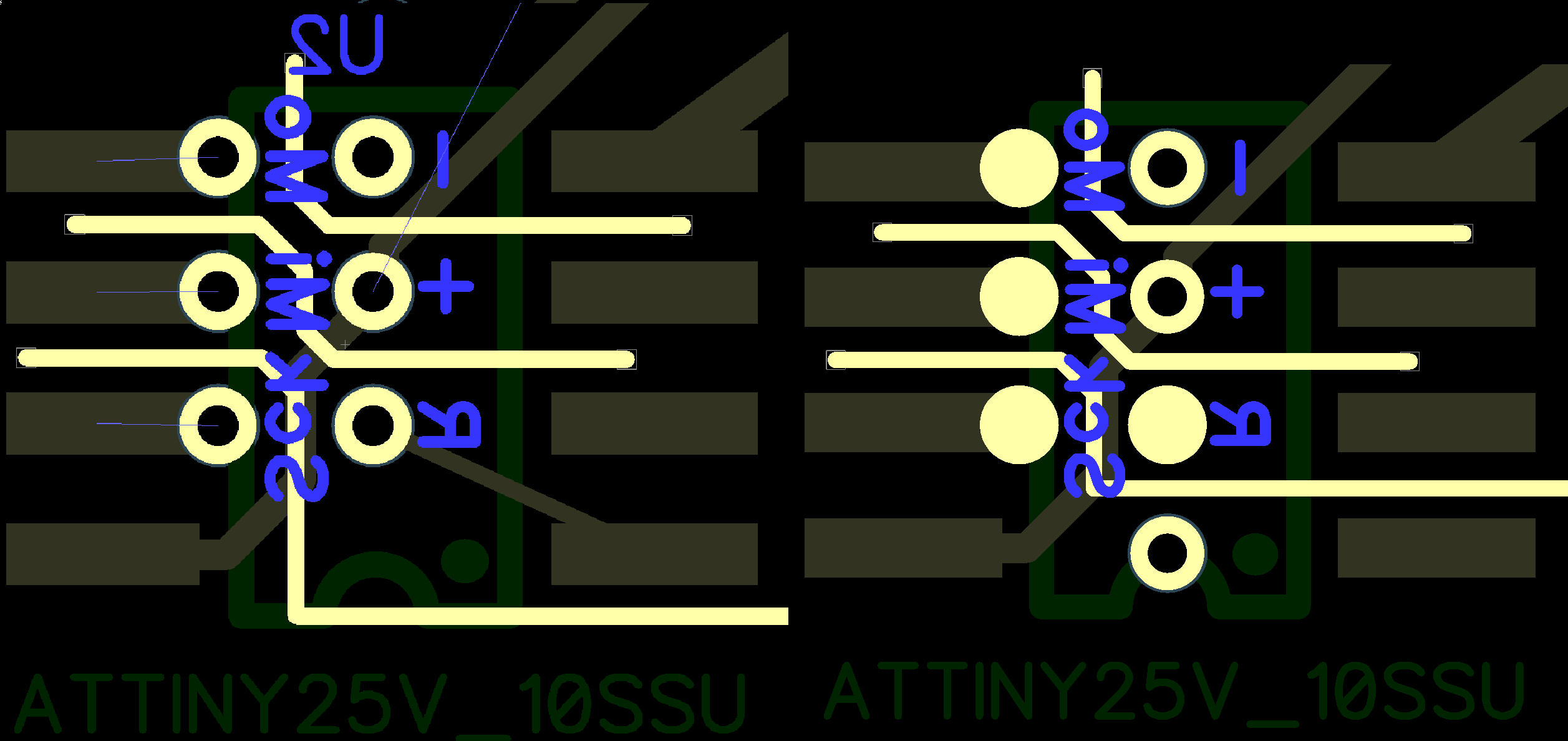
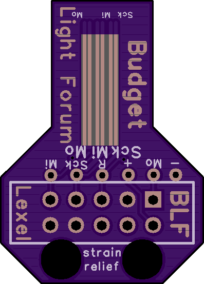
rearranged pins to fit MCU pins arrangement better than original v1.0 had
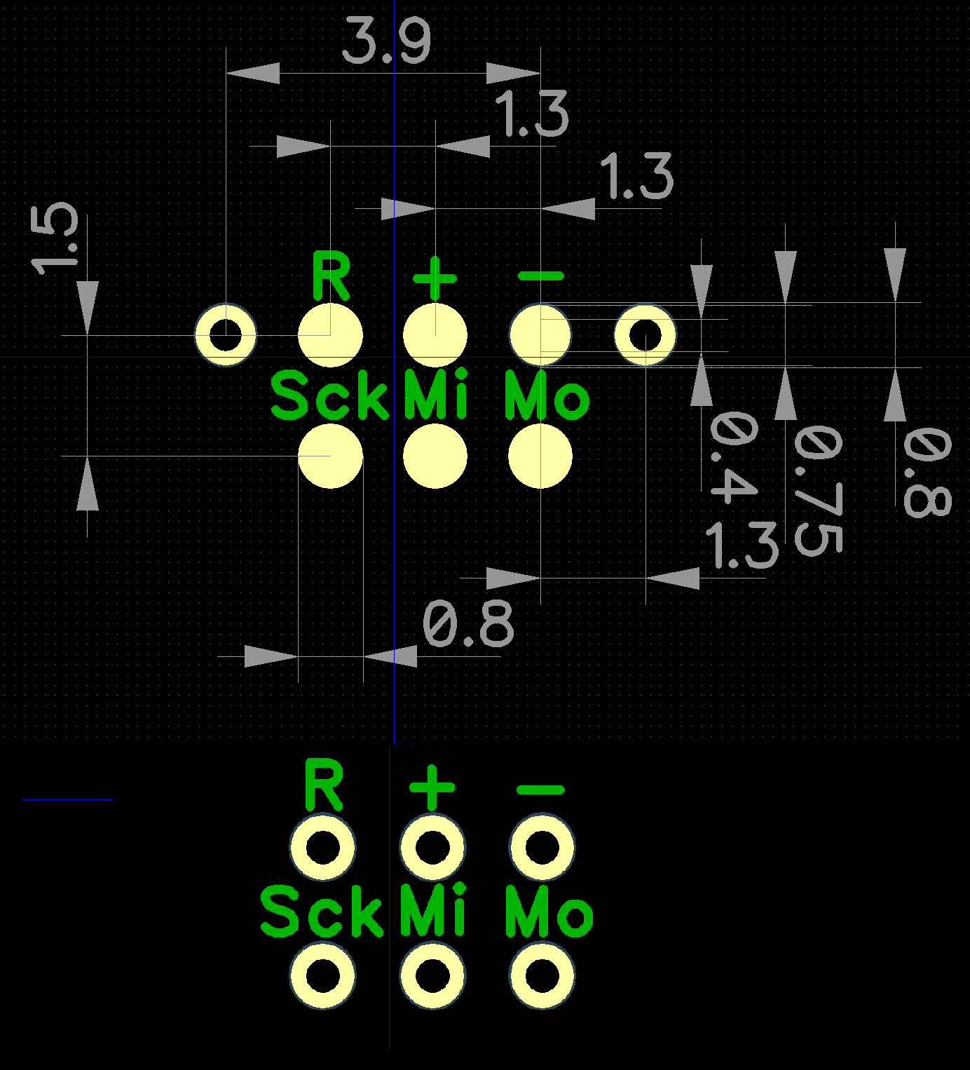
pitch is 1.3mm so with 0.8mm 6 mil traces can be routet between them, also added a variant with just 6 viases if this can be fitted on driver
basically only 2 connections need to be viases to align the pogo pins
improvement machanically on key
2 traces on the pogo pin board to self align it by the solder
increased pad size on driversfrom 0.6mm to 0.8mm, to compensate wrong aligned pogo pins
length of the solder traces on board reduced as some flux went in the pogo top, can be solved with alcohol but more distance is better
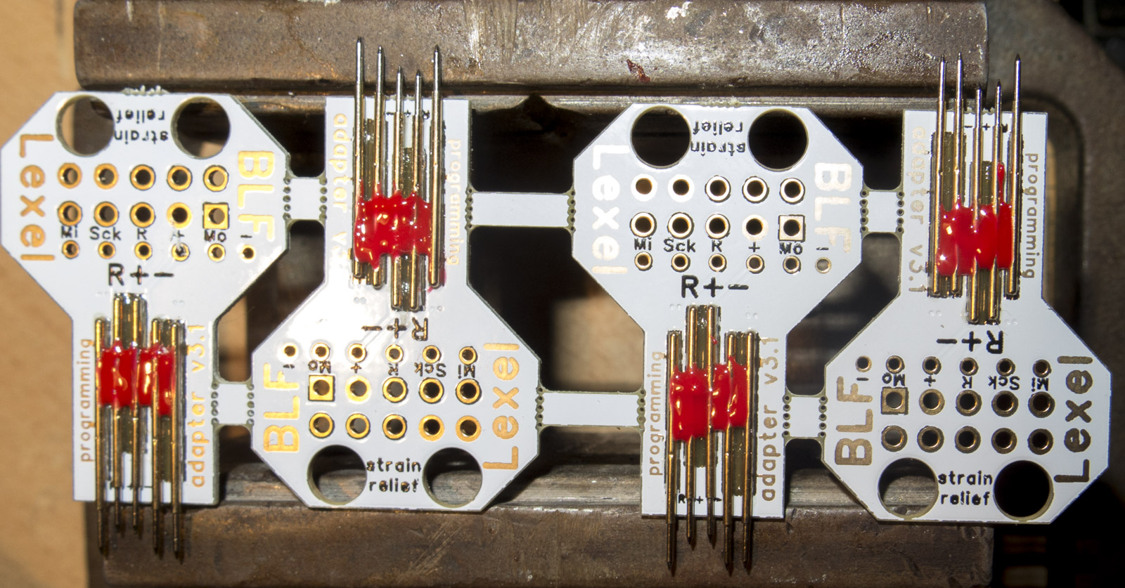
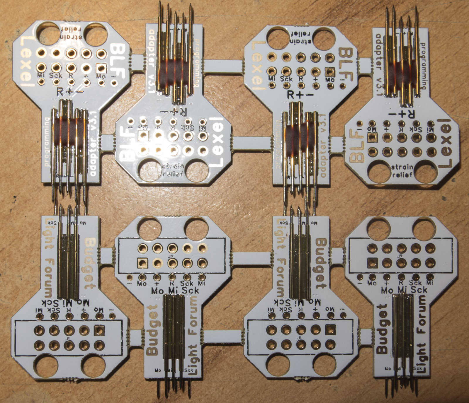
Added a key head for easier handling
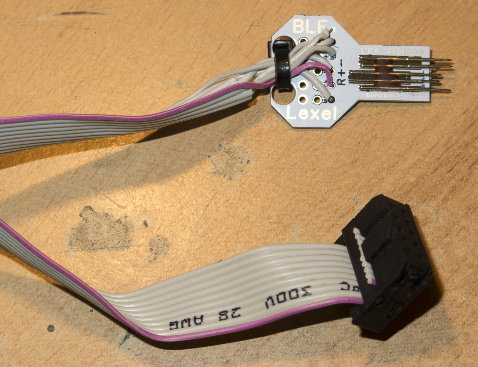
added 2 holes to use a wire strap to secure the programming wire
on drivers
cleared solder mask around alignment pins as sometimes the solder mask covers the whole hole (not Oshpark but cheaper fabs in China)
0.8mm Oshpark board a bit more thick than anticipated, 0.1mm added on drivers port pad distance between the 2 layers
Picture of v1.1 key on V1.0 board, pin alignment does not work (no self centering while reflow) on the small 0.6mm pad
I moved the pins further below, because having solder paste next to the pin hole is no good idea
also the solder mask on the outer alignment viases is blocking the holes, so added solder mask around them
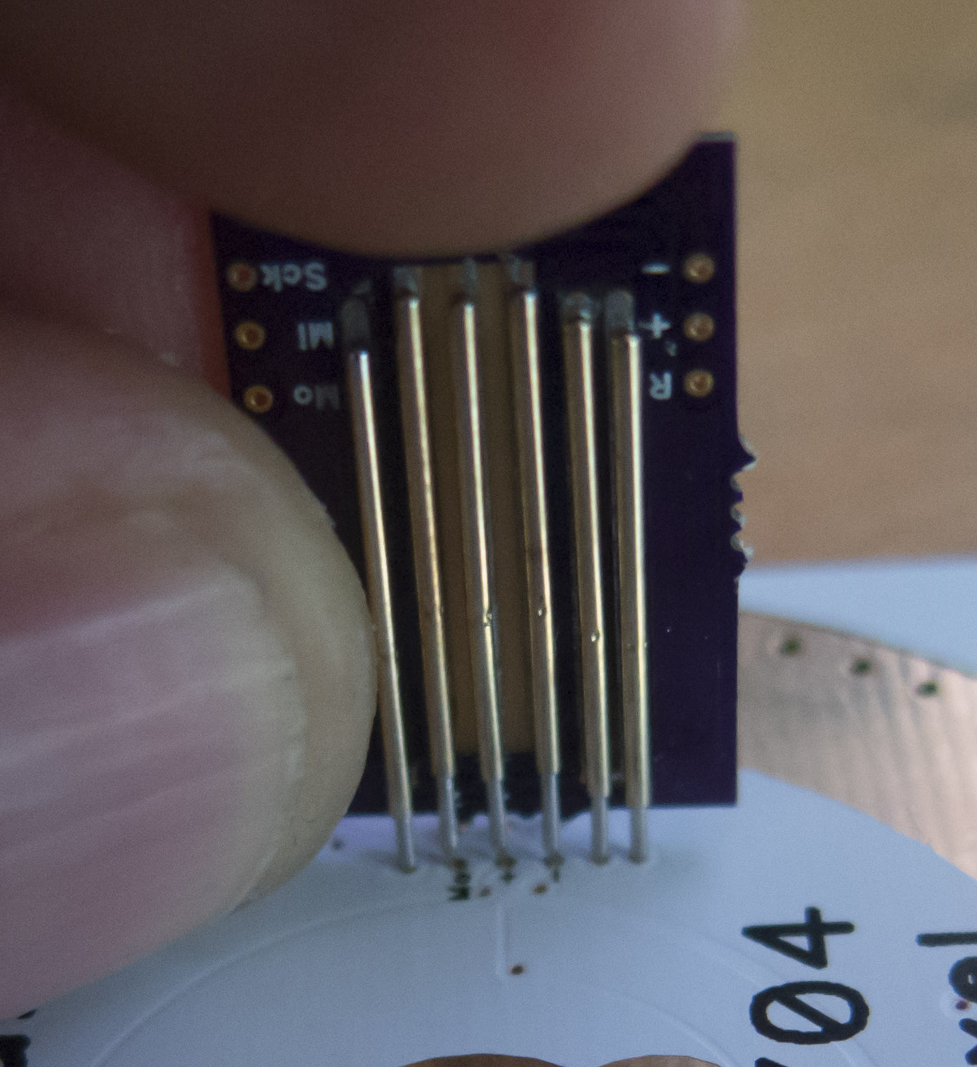
Those are 0.5mm thick pogo pins with a 1.3mm pitch, not the 1.02mm with 2.54mm pitch
I also got my final revision 3.2 also launched now on Oshpark
the v3.1 boards i have here can be used but with some advise
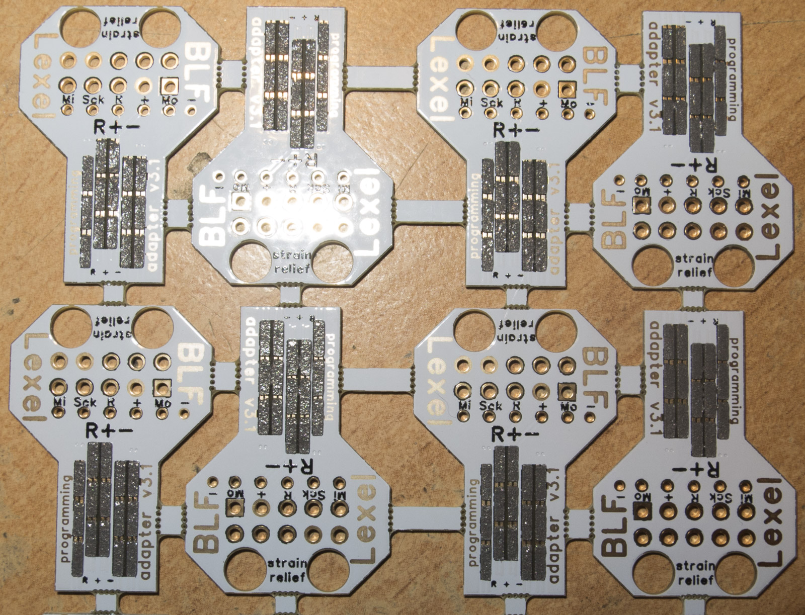
I got made 120 boards where the 10 pin header wont work when used with 1:1 wire, 4 traces need to be swapped out
and solder connection markings do not fit
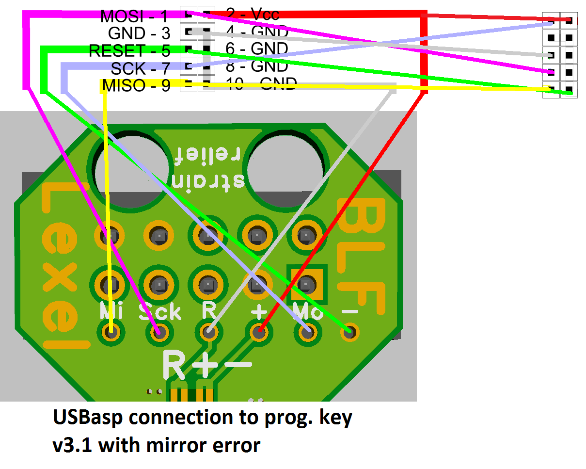
the pins are mirrored because I made an mistake looking in my program on drivers bottom which auto mirrors
Order in 2OZ for 0.8mm board thickness from Oshpark!
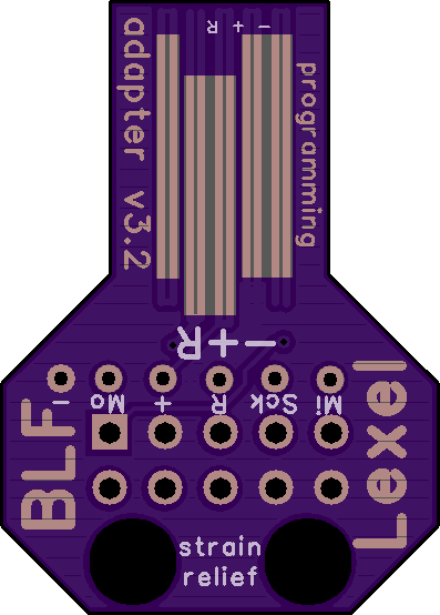
https://oshpark.com/shared_projects/o1pUPNqt
I got some that cant use the header as they were produced mirrored
Production
applying solder paste one side
soldering pins to it and applying thermal glue for 2. side reflow
Both sides soldered, fine alignment of the pind with soldering iron carefully after that picture
final key with soldered wires not connector
Nice concept.
Any chance for a short description?
![]()
I really like the idea of an on-the-fly programming stick, I just can’t follow from the pictures:
For which mcu is it, why 9 pogo sticks, how far are the sticks apart (center to center), why are the sticks on a different height, how is the programmer connected to the key?
Much appreciated.
It works as it is, plese comment only if you have further improvements or want to discuss details
If you want to get the footprint for your design program I can mail it to you (Gerber or Diptrace libary)
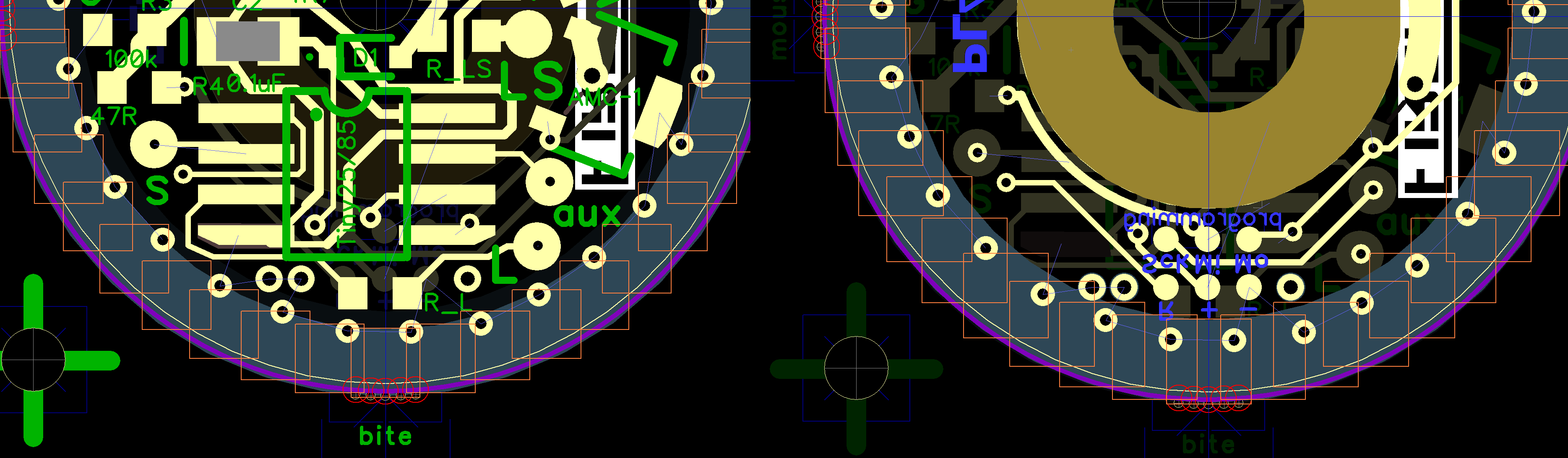
3 orientation pins are sticking out further and rest in viases
6 Pins are connected on the driver design to the MCU pins for programming, any MCU that can be flashed with USBASP programmer
perfect
thanks for adding the picture with the dimensions
Nice!
How do you reflow the pogos, with hot air? IR? Ofen? Plate?
Glad I stumbled across this. I am working on a driver for the BLF Ultimate Lantern, and planned on adding reprogramming vias. I had no guidance on spacing or location, but it makes sense to make it compatible with this device. I know you are open to comments here, but any idea when this design will be complete? Also, I missed why the center to center spacing is not symmetrical for the hole on the far left. Is that part of the keying?
Pardon my ignorance, but what kind of lights or drivers is this suitable for or compatible?
Why 3 orientation pins instead of 2?
Also, for making it even more compact, what about having only 6 pins total and making some or all of them vias? For people who don’t have a key, vias are a lot easier to use than pads.
It’d be awesome to get a standardized BLF programming layout and key, so I hope to maximize the amount of drivers it can fit on while minimizing the barrier to entry.
Will you consider to put an ISP programming 2.54mm pinhead at the top of the key?
Does it make a difference, if the pin pitch is 50Thou or 1.3mm ?
For pogos on pads I think no.
But for pogos in vias it adds up:
5 pins = 5 distances
5*0.03mm = 0.15mm
So the outmost guiding pins are 0.15mm off IF the pcb manufacturer set the 1.3mm to 50mil.
Edit: just saw you have variable pin pitches
(could be a possible trap to fit the key int the vias and it’s also possible that I am overthinking)
Edit:
Die Maßangabe
0.85 and 0.91
What is it, a tolerance?
I think he used three orientation pins is to prevent reverse connection.
making all programming pins viases blocks a bunch of area on small drivers likely make routing very hard if its packed with componets, with pads you are way more flexible, as they block that area only on one side
It is possible to remove one centering via where now 2 are, you can design the driver with just 2 centering viases
also tolerances play a big hole making it 6 viases, 6 pads are far more tolerant if pogo pins not aligned perfectly
0.91 is the solder Mask I cleared around the viases, fabs often fill the viases with solder mask if you have no clearance around them
also the fab has to produce from your gerbers there is no converting pitch 1.3mm to 50mil
also the 1.3mm was choosen so you can route a 6mil trace between the pads and pads and viases, if its 1.27mm you can not route it with the nessesary clerarance withoput making the pad and viases smaller
here an example
Agreed, no orientation pins required. This is not a tool for the un-initiated, placing it the right way is hardly rocket science.
The point of this is to facilitate ISP with the latest MCUs where external clips are not an option (no leads). Which was always a rickety arrangement, involving USBasps, headers, cables, clips etc.
Best if all pads are also vias, so self-locate.
Six pads/vias. No more. No extra “orientation” stuff, just obvious silk screen.
Frankly, this was all sorted out long ago, it’s not new, e.g. just google “pogo pin isp programming adapter” and follow the (unofficial) standard.
Then do it.
OK so pogo pins with a bit larger head, pitch 1.3mm
but the inofficial standard bases on 2.54mm pitch, then we make it larger again
Problem with this is often below the MCU is something that blocks it like spring pad or so
here a driver example
OK, I agree 0.1 inch spacing is quite large by modern standards.
But what is available at smaller pitch ? The smaller you go, the more esoteric the components become, and the method of assembling them. An FR-4 key is as basic as it comes, maybe a bunch of pins glued together with e.g. Sugru even worse. When I started this idea I suggested a 3D printed matrix to assemble things, I still think that’s the way to go for something reliable. But lets see where this goes.
Bottom line is that a standardised ISP connection on the accessible face of the driver is very desirable. If it can be connected with a click or a twist, even better. But a simple pressure contact with half a dozen pins on a standard pattern would be fine, even if only a couple are vias, for location.
this is why someone wrote me to use 2 traces so the pins self center themselfes while reflowing
with this method no worrying about it, just put solder paste and pins on the board and reflow it, perfectly aligned
on most of my smaller driver designs going with a 6 viases programming footprint wont work, because its literally packed by tons of traces on top, and also the spring pad and other stuff will limit it a lot where you can place the programming port
Problem with this is often below the MCU is something that blocks it like spring pad or so
here a driver example with 24mm size, not as small as a 17mm for example, I had no idea if its even possible to get the 6 viases on my 17mm or not
I thought about it why not make a 7 pin pattern which works for pads and viases, and modified it a bit
I have no experience with this so I can’t comment on the design, but being able to program the driver without having to remove anything is just awesome Lexel. :+1: :+1: :+1: ![]()
I second this comment.