Ok, makes sense. Thanks for the explanation.
Hey, I like my MM15vn and X60vn! ![]()
I probably can’t justify spending as much as I did for the X60vn for another flashlight ever again. That was too much, but it’s a really good flashlight.
Famous last words. Unless you’ve got a really good therapist (or a SWMBO intervening) your drooling over the next super-light will short out your keyboard causing this to happen anyway. You cannot resist- ALL will be assimilated :bigsmile:
And I like shrick’s mention of lower modes being useful; something this ‘newbie’ has had to learn the hard way. Good doing business with RMM, never had better value and service from anyone anywhere.
Phil
I won’t post links, but I wasn’t referring to Vn lights. I saw some custom machined EDC lights recently, and they were going for $400ish tricked out with basically LMH drivers. Jeeze. I get why they’re so much… you know, Because they’re hand made, but I could never justify dropping that.
Has anyone measured the standby current draw of the Qlite e-switch?
I’m modding cheap led lantern that only has a e-switch, plan to use 2x 219C and 4x7135 Q lite driver.
Thanks!
Hi,
I have a couple of the FET+7135 boards plus the parts kit, but is there something/somewhere shows the parts layout for building this board?
I’ve seen a couple of pics on the original thread, but I’m looking for something that identifies which part goes where along with orientation where it matters.
Thanks,
Jim
EDIT: I just found Tom E’s pic in post #149 of this thread:
Is that the correct layout?
Edit2: the layout in that post looks completely different to the PCBs I have :(!!!
Didn’t RMM label the parts he shipped to you? He usually does
This what you are after?
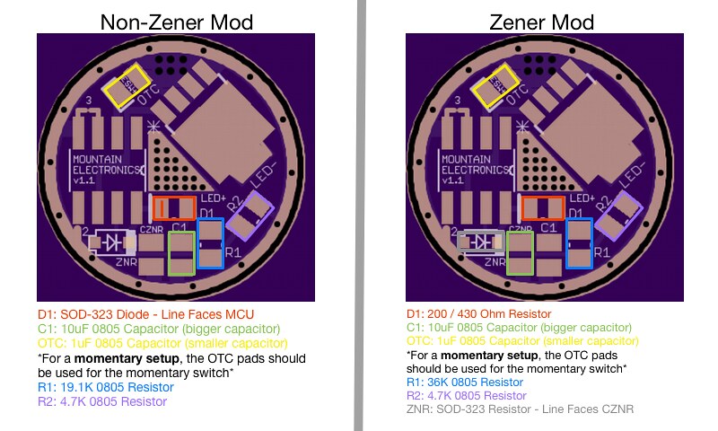
Hi,
Yes, that’s what I was looking for.
1) So for the non-zener mod configuration, is that diode position under/below the MCU not populated?
2) Which position is MCU pin #1? Is it the one with the *?
3) Where do the + and - emitter leads actually go? Is the + that grid of holes and is the - the tab of the FET?
Thanks!
Jim
Edit: The boards I receive are different… looks like they are 1.0 :(….
1; correct
2; correct
3; see 1 or 2 ;)
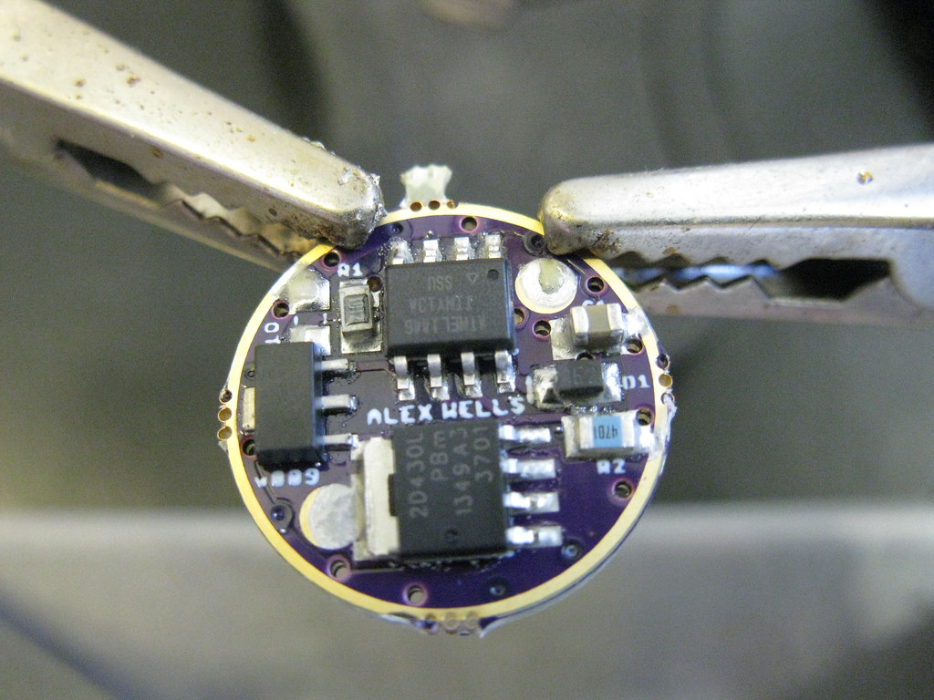
I think you need to take a picture of your boards! H)
..sorry, obviously the picture I posted is not the Fet+7135 board.
I have a populated Wight Fet+7135 that I can u/load a picture of if it helps.
Here’s what I got from RMM:
and the driver board itself:
FYI, I think that I was able to get one of the boards working, kind of following the layout you showed. I guess that the overall layout (or at least parts) didn’t change much between the FET and the FET+7135 drivers?
Jim
EDIT: In my case:
D1 - the diode in the package - line was towards 7135
R1 - same as yours
R2 - same as yours
C1 - same as yours
OTC - same as yours
ZNR - not populated
emitter + ==> plated area with bunch of holes
emitter - ==> tab of the FET
EDIT 2: RMM was able to flash the MCU with a tweaked version of the BLF-A6 firmware.
Sounds like you have got it under control now :)
The Wight Fet+7135 board layout is different again;
Just to cut down on the confusion and the time RMM spends answering questions it seems like it would be worthwhile including a high resolution photo or drawing of the populated board with each board type that RMM offers. If not shipped as part of the build kit then include it as one of the photos in the board listing so it can be downloaded and printed out by board and kit purchasers. If the board can be assembled with different options then include a photo/drawing for each option with clear labeling.
The old Heathkits included very complete documentation so in general even a novice electronics assembler could build their boards.
Just a suggestion.
I took this picture earlier today:
It is the MTN-17DDm FET + 3175
I used to think I would get some kinda (weirdo) ZEN satisfaction assembling my own drivers too, yeah O.K. that was short lived (F-bombs aside):bigsmile: Now I just keep a GOOD supply of FET’s and 7135’s at hand, because that’s what goes when I see the tell tale spark, sliver of smoke, dim erratic modes, or no modes at all. :_( Got real good at replacing them!! ![]() The rest I leave to the Pro, King of stacking chips, Richard!!
The rest I leave to the Pro, King of stacking chips, Richard!!
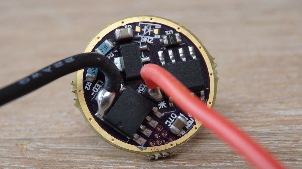
Thanks. I think that’ll be helpful, but could you do a pic w/o the emitter wires?
I have another one to build and I can take a pic of that w/o wires if not.
Jim
Building these is much easier than stacking chips!
In my case I reflowed the small components first then the FET and MCU.
To reflow, I used solder paste & put the board on top of a 1/4 inch copper plate and heated that from underneath w a small torch.
thijsco19’s pic is much, much clearer, so use that for clarity, but here’s an annotated pic of a populated board without the emitter leads: