|
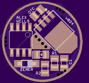
Watch out for Zener build compatitibility issues in this version. There is a simple workaround for the current version (v024), see post #319 here for details. Also in post #319 and 320 you’ll find two different revised WIP board layouts which should both remove the need for any workarounds. |
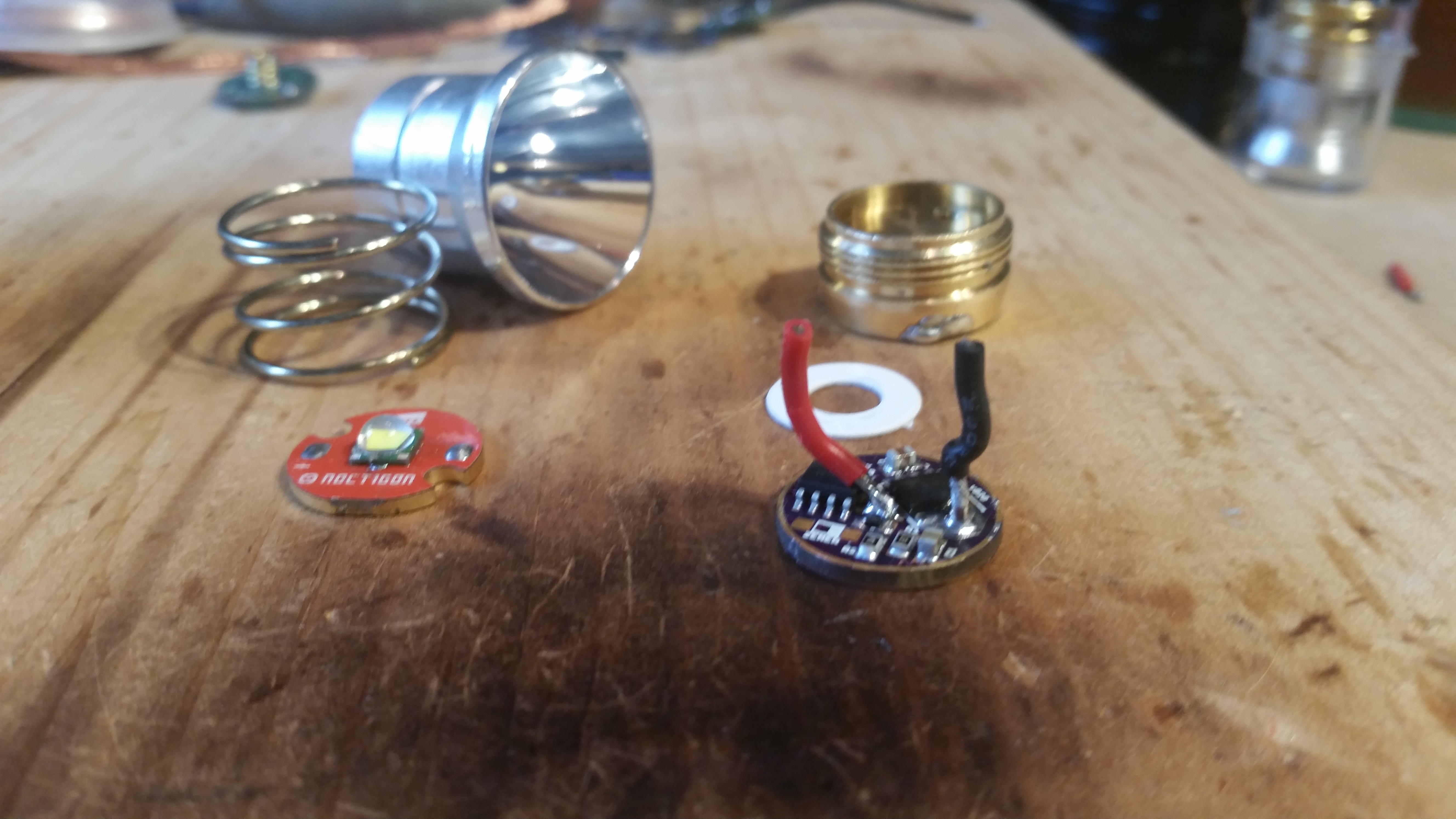
Here is a high power single sided FET driver. From my limited testing, fresh battery performance is similar to a regular BLF17DD. The driver is Zener ready. Note that this driver is not intended for a DPAK FET such as the (unavailable) Vishay 70N02; instead it uses an LFPAK56 (AKA Power-SO8) type FET like PSMN3R0-30YLD.
The primary goal for this driver was to create something which fit better in flashlights with retaining rings. The Supfire L6 is an example, it’s huge retaining ring prevents the use of two-sided driver. To that end this driver has absolutely no components on the spring side.
Secondary goals:
- 1mm component keepout around the edge
- Easy to build: reflow or hand solder easily (large 0805 sized pads)
Zener ready…sort of. See note at top of OP.- Offtime ready
- Put my mark on it


More info:
- All the above notwithstanding, this driver is still simply a derivative of the 17DD+7135 [WIP] driver I’ve been working on over here. The layout of the entire top half of the driver is the same.
- As of v024 I used a 1.5mm thick GND ring on top and bottom where possible via polygons. Cereal_killer’s post #44 in the DD+7135 thread got me thinking and this is where I’m at for now. There is still only 0.5mm exposed. I feel like we’ve got plenty of strength now! Good thinking C_k.
- D1/R3 is only designated through a triangle and a white line marking the cathode. The triangle has been updated slightly since v020 because it was too large and not sharp. The cathode mark was not present in v020 but should be present in v024.
- Like the DD+7135 driver, this driver does have a reverse-polarity protection diode but bypasses the diode for the voltage divider. Due to this we are able to use any diode desired. Ideally we use a protection diode with an extremely low Vf in order to maximize gate voltage!
- The exposed spring pad is 8mm. Scraping will reveal up to 11mm of copper. GND does not start until 15.5mm.
I’ve now built two of these using this component list:
C1 - 4.7uF [GRM21BR61E475KA12L]
R1 - 22k 0805
R2 - 4.7k 0805
D1 - SOD-323 & SOD-723, assorted
OTC - 1uf [C2012X7R1E105K125AB]
MCU - ATTINY13A-SSU
FET - PSMN3R0-30YLD
I have not assembled one with a Zener, but the pads are intended for an SOD-123 sized component. You may wish to use a higher capacity C1 than what I used, 10uF is fine as well. I used what I had on hand at the time. Based on some recent testing I did 3uF definitely does not work, 5uF and 4.7uF do work. I never tested 4uF. My 22k R1 replaces the 19.1k R1 due to the change in how the divider hooks up to B+. 22k is not guaranteed to be perfect, but it’s close enough for me and for now. Other more prolific modders may identify a closer value which appeals better. I’m happy with the cutoff I got from those components and a stock STAR offtime v1.3 firmware.
In testing with an OG XM-L of unknown bin I repeatably achieved 9A+ at the tailcap with a freshly charged Samsung INR18650-15M. The firmware uses JonnyC’s turbo rampdown mod, so current quickly falls of course. Here’s the dropin guts for that:
Finally, here are the OSH Park images.
17mm version:

https://oshpark.com/shared_projects/TrEN1wLB
20mm version:
w/ 1mm exposed copper on GND rings.


https://oshpark.com/shared_projects/YeNzvLPx
Credits to those who got the ball rolling on this stuff such as Mattaus and comfychair. And to the East-092 of course. ![]()